
Basic Circuit
Index 276
EXCLUSIVE_OR
Published:2009/7/5 20:25:00 Author:May
gate combines both pulses at output、Values shown for R and C will double frequency of 800-μS-wide inρut pulses having repetition rate of about 130 ρer second.-K.R.Brooks,Pulse Rate Doubler Wireless World,Aρril 1976、ρ 63 (View)
View full Circuit Diagram | Comments | Reading(806)
LOW_CAPACITANCE_DRIVER_FOR_RAM
Published:2009/7/5 20:19:00 Author:May
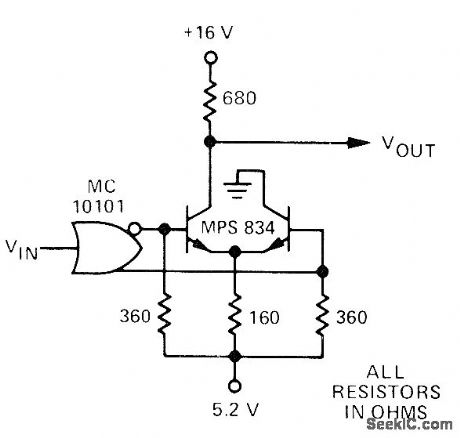
Suitable for data input lines of memory system operating from 16-V supply with memory input logic swing of 16 V. Used with Motorola 1103 dynamic RAM for which transition times of data input signals should be 20 ns to give maximum memory speed. Suitable for maximum capacitances per line as high as 20 pF.-D. Brunner, A MECL 10,000 Main Frame Memory System Employing Dynamic MOS RAMs, Motorola, Phoenix, AZ, 1975, AN-583, p 13. (View)
View full Circuit Diagram | Comments | Reading(605)
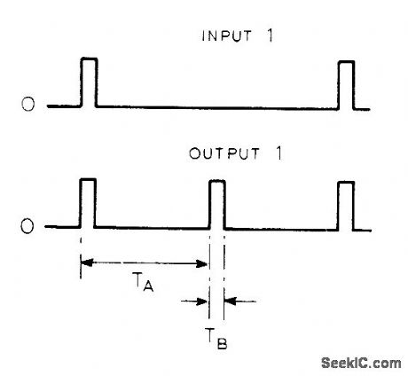
PULSE_DOUBLER
Published:2009/7/5 20:17:00 Author:May

Generates pulses at twice pulse input frequency. Input pulse at first monostable of 74123N makes it run for time TA. Negative edge, terminating TA, triggers second monostable which runs for time TB. If TAequals haff of input period and TB equals width of input pulse, desired result is aehieved wherein additional pulse is generated between input pulses. (View)
View full Circuit Diagram | Comments | Reading(1435)
MEMORY_SAVER
Published:2009/7/5 20:16:00 Author:May

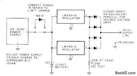
Standby battery takes over automatically during power failure to prevent memory loss. Use any rechargeable battery that can handle load. Connect one LM340-5 regulator in circuitfor each 1.2A of load current drawn by circuits to beprotected. In normal operation, output diodes are biased off by slightly higher voltage from computer. During power failure,they are switched on by removal of bias. Current is then supplied by battery. Output should be loaded with resistor drawing ahout hatf of trickle-charge current, so battery has small continuous current flow and stays charged.-C. R.Carpenter, Protect Your Memory Against Power Failure, Kilobaud, March 1978, p 73. (View)
View full Circuit Diagram | Comments | Reading(822)
AF_MULTIPLIER
Published:2009/7/5 20:11:00 Author:May
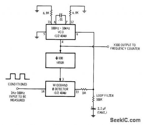
Multiplies 1-100 Hz input signal by 100 to permit measuring frequency with ordinary counter. Half of 4046 PLL is connected as 100-10,000 Hz VCO whose output is divided by 100 in 4518 dual divide-by-10 counter for comparison with input signal in other half of PLL connected as wideband phase detector.Output of detector goes to loop filter and to VCO for locking VCO at 100 times input frequency.-D. Lancaster, CMOS Cookbook, Howard W. Sams, Indianapolis, IN, 1977, p 364-366. (View)
View full Circuit Diagram | Comments | Reading(1367)
73333_MHz_ON_THIRD_OVERTONE
Published:2009/7/5 20:03:00 Author:May

Simple crystal oscillator circuit requires only one tripler for multiplying to 220-MHz amateur band.Mode suppression is provided by 10-μH coil which, with 4.5-pF capacitance of crystal holder, is series resonant at 24 MHz.-H. Olson, Frequency Synthesizer for 220 MHz, Ham Radio, Dec. 1974, p 8-14. (View)
View full Circuit Diagram | Comments | Reading(981)
DOUBLER_FOR_TACHOMETER
Published:2009/7/5 19:58:00 Author:May

Frequency of input from tachometer is doubled by charging and discharging of C1 to reduce ripplein DC output voltage of tachometer circuit. Opamp 2 provides bias current for opamp 1, while Q1 drives large load currents and provides DC level shift required for bringing output voltage to zero when input frequency is zero.-T. Frederiksen, Frequency-Doubling Tach Operates from a Single Supply,EDN Magazine, June 5, 1977, p 208. (View)
View full Circuit Diagram | Comments | Reading(1424)
SINE_WAVE_DOUBLE_
Published:2009/7/5 19:51:00 Author:May

Frequency of sinusoidal input signal VS is doubled to give sine-wave output with total harmonic distortion less than 0.6%,With input of 4 V P-P at 10 kHz、output is1V P-P at 20 kHz. X and Υ offset adjustments are nulled to minimize harmonic content of out-put.-″PhaseˉLocked Loop Data Book,''Exarlntegrated Systems,Sunnyvale,CA,1978,p 9-16. (View)
View full Circuit Diagram | Comments | Reading(730)
FET_DOUBLE
Published:2009/7/5 19:40:00 Author:May

Siliconix E300 matched FETs are connected as common-gateamplifiers in blanced push-push circuit giving up to 100% efficiency as frequency multiplier in UHF range.series-tuned output trap L2C8 increase rejecttion of third-orde harmonics to greater than 70dB.Positive bias of 0.5 V is applied to FET gates to permit inclusion of balance control R2,Gainof doubler is about 1 dB.-''Analog Switches ''and Their Applications,''Siliconix、Santa Clara,CA、1976 p7-52 (View)
View full Circuit Diagram | Comments | Reading(1236)
SQUARE_WAVE_DOUBLER
Published:2009/7/5 19:18:00 Author:May
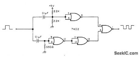
Circuh locks onto both rse and fall of input square wave, to give identical square-wave output at doubled frequency. For high input frequencies, use smaller capacitance values.-Circuits, 73 Magazine, April 1977, p 164. (View)
View full Circuit Diagram | Comments | Reading(1943)
MULTIPLIER_DIVIDER
Published:2009/7/5 19:13:00 Author:May
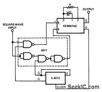
Choice of values for R and C determines multiplication or division factor acting on square-wave input frequency. 0utput of 4013 flip-flop sets gates of 4011 to steer input clock pulse of RCA CD4047AE mono MVBR to proper inputs. When rising edge of input triggers mono, Q output of mono goes high and switches flip-flop, preparing mono to accept falling-edge trigger. Since 4047 locks out inputs until ittimes out, mono triggers only on first falling edge occurring after its output goes low. Mono pulse length is about 2.5RC. With 60-Hz input clock, mono pulse length less than 8.33 ms allows triggering on every transition, to give 120-Hz output.-P. A. Lawless, One-Shot Forms Frequency Multiplier, EDN Magazine, Aug. 5, 1978, p 72. (View)
View full Circuit Diagram | Comments | Reading(1450)
PLL_MULTIPLIES_BY_10
Published:2009/7/5 3:55:00 Author:May

Used with frequency counter to measure very low frequencies. Two such circuits can be cascaded to give multiplication by 100. Requires +5 V and +12 V supplies.-H. S. Laidman, Upgrading Inexpensive Counters, CQ, Aug. 1975, p 16-22. (View)
View full Circuit Diagram | Comments | Reading(622)
WIDEBAND_DOUBLER
Published:2009/7/5 3:46:00 Author:May
AC-coupled multiplier block is connected in squaring mode to provide second harmonic of input frequency with no tuned circuits. Circuit operates over wide bandwidths without adjustment. Output is low-distortion sine wave; total harmonic distortion is typically 1%. Output can be taken from pin 2 or 14, depending on phase desired. Circuit will work with R7 grounded, but offset adjustment can be used to minimize distortion. Maximum operating frequency is several megahertz.-W.G. Jung, IC Op-Amp Cookbook, Howard W.Sams, Indianapolis, IN, 1974, p 258-259. (View)
View full Circuit Diagram | Comments | Reading(593)
PUSH_PUSH_DOUBLER
Published:2009/7/5 3:39:00 Author:May
Usefui in VF0 output circuits where oscillator operates at half output frequency of doubler. Circuit helps reduce osdllator instability during load changes while having about same efficieney as straight amplifier. Uses two sections of RCA CA3028A differential amplifier as doubler (U1C is not used).Values of tuned circuit depend on frequency, which can be up to 120 MHz.-D. DeMaw, Understanding Linear ICs, QST, Feb. 1977,p 19-23. (View)
View full Circuit Diagram | Comments | Reading(643)
500_5000_Hz_SQUARE_WAVE_DOUBLER
Published:2009/7/4 22:27:00 Author:May

Circuit shows virtually no deviation from 50% duty cycle over entire frequency range. Four NOR gates in CD4001AE IC form edge detector that presents negative pulse to 555 IC timer on both rising and falling edges of input square wave, to achieve frequency doubling. High-gain 741 opamp amplifies any difference between DC level at timer outputand reference equal to half of supply voltage, to send correction voltage to pin 5 of timer for forcing output to 50% duty cycle.-L. P. Kahhan, Frequency Doubler 0utputs Square Wave with 50% Duty Cycle, EDN Magazine, June 5, 1977, p 211-212. (View)
View full Circuit Diagram | Comments | Reading(1903)
PROGRAMMABLE_PLL_SYNTHESIZE_MULTI_PLIE
Published:2009/7/4 22:14:00 Author:May

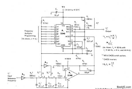
Uses programmable timer/counter A 1 as vco for generating frequencies both aboveand below that of square-wave reference Phase-Locked output frequency is not direct multiple of reference frequency. 2240 can lock on programmable multiple or on subharmonic reference. For values shown, phase-locked loop is locked through common frequency submultiple of 10 Hz, to give sampling rate of 10 Hz for reference input.-W. G. Jung, IC Timer Cookbook, Howard W. Sams, Indianapolis, IN, 1977, p 220-224. (View)
View full Circuit Diagram | Comments | Reading(567)
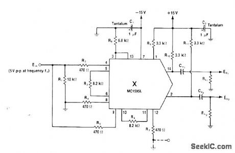
BROADBAND_LOW_FREQUENCY_DOUBLER
Published:2009/7/4 22:05:00 Author:May

Motorola MC1596G balanced modulator functions as frequency doubler when same signalis injected into both input ρorts (plns 1 and 8),Doubling occurs audio range and up to about 1 MHz.-R.Hejhall,″MC1596 Balanced Modulator,″Motorola,Phoenix、AZ,1975,AN-531,p 10 (View)
View full Circuit Diagram | Comments | Reading(961)
245_MHz_TO_147_MHz
Published:2009/7/4 21:56:00 Author:May
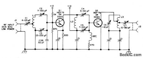
UsesQ1 as tripler to73.5 MHz for frequency-modulated input of 24.5MHz, and Q2 as doubler whose output tank is tuned to 147 MHz by C6 and L3. Output is about 200 mW of RF. L1 is 20 turns No. 26 with center tap, on 0.5-cm form. L2 is 8 turns No. 22 on 0.8-cm form. RFC is 25 turns on 0.5-cm form. Article covers troubles likely to be encountered.-B.Hoisington, Frequency Multiplication the Easy Way, 73 Magazine, Oct. 1973, p 69-71. (View)
View full Circuit Diagram | Comments | Reading(594)
DOUBLING_150_MHz
Published:2009/7/4 21:43:00 Author:May
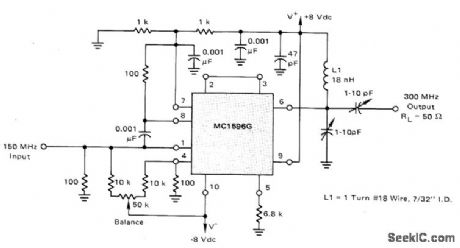
Motorola MC1596G balanced modulator is connected for doubling at RF and UHF.With output filtering shown,all spurious outputs are at least 20 dB below desired 300-MHz output. Suppression of spurious outputs is poorer for higher input frequencies,being only 7 dB down for 400-MHz output, but performance is still superior to that of conventional transistor doubler.-R. Hejhall, MC1596 Balanced Modulator, Motorola, Phoenix, AZ, 1975, AN-531, p 10. (View)
View full Circuit Diagram | Comments | Reading(539)
DOUBLING_200_MHz
Published:2009/7/4 21:30:00 Author:May
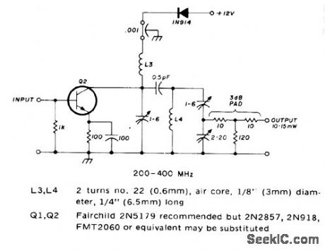
Recommended for use with VHF/UHF converters having inptuts of 180 to 220 MHz, with 5-10 mW output. Diode in series with power supply prevents damage if polarity is reversed.-J. Reisert, VHF/UHF Techniques, Ham Radio, March 1976, p 44-48. (View)
View full Circuit Diagram | Comments | Reading(1019)
| Pages:276/471 At 20261262263264265266267268269270271272273274275276277278279280Under 20 |
Circuit Categories
power supply circuit
Amplifier Circuit
Basic Circuit
LED and Light Circuit
Sensor Circuit
Signal Processing
Electrical Equipment Circuit
Control Circuit
Remote Control Circuit
A/D-D/A Converter Circuit
Audio Circuit
Measuring and Test Circuit
Communication Circuit
Computer-Related Circuit
555 Circuit
Automotive Circuit
Repairing Circuit