
Basic Circuit
Index 260
NICAD_BATTERY_ANALYZER
Published:2009/7/6 5:50:00 Author:May

Because NiCad batteries maintain a constant output voltage, it is difficult to determine how much of the battery's charge remains. The circuit provides a way of determining the capacity of a battery by draining it at a preset current to its depleted voltage of 1 V/cell. Measure the discharge time of the cells and perform a simple calculation to obtain the battery's capacity.
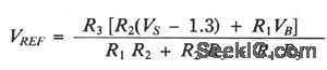
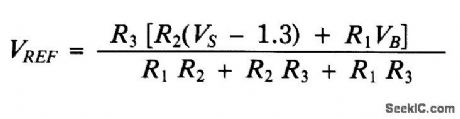
Set the drain current(ID) to 0.5C (C = battery capacity in mA/hr) by selecting an appropriate value for R4. Choose R5 such that: ID x R5 = 1 V. VREF is set so the comparator turns off the drain current and timer when the battery reaches its depleted voltage, VB (usually 1 V/cell). You calculate VREF as follows:
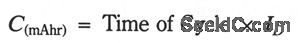
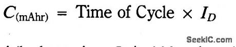
With the battery in place, activate the circuit by grounding VREF with the momentary switch. The battery drains at ID until it reachesVB, turning off the drain circuit and the timer. Hysteresis keeps the circuit from restarting. Determine the battery's capacity using the following equation:
The circuit shown tests 4.8 V, 180 mA/hr batteries. ID is 100 mA and VB is 4 V. (View)
View full Circuit Diagram | Comments | Reading(596)
“HEE_HAW_TWO_TONE_SIREN
Published:2009/7/6 5:47:00 Author:May
The circuit uses two gates of a 7400 IC cross-connected to form an astable multivibrator driven by the 1-pulse per second output of the digital clock IC. The hee-haw circuit has a low frequency astable modulator added to make a selfcontained European-type siren. Tone and rate can be varied as desired by changing capacitor values. If the tone is too harsh, a simple R-C ftlter will remove the harmonic content-the multivibrator output is almost a square wave. With the resistor values shown, no start-up problems occur; but if the 2.2 k or 2.7 k resistors are changed too much, latch-up can be a problem. (View)
View full Circuit Diagram | Comments | Reading(2893)
RUMBLE_FILTER
Published:2009/7/6 5:46:00 Author:May

Used when rumble from cheaper turntable or record extends above 100 Hz, causing disconcerting out-of-phase loud-speaker signals, Circuit is based on fact that human ear is not sensitive to directional information below about 400 Hz, making it permissible to remove stereo (L – R) signal at low frequencies and thus remove stereo rumble without losing stereo separation. Emitter-followers feed high-pass filters having 200-Hz breakpoint frequencies and Butterworth characteristics. Attenuation of filter is 12 dB at 100 Hz. Filter circuit can be disabled by placing switch between points P and Q.-M. L. Oldfield, Stereo Rumble Filter, Wireless World, Oct. 1975, p 474. (View)
View full Circuit Diagram | Comments | Reading(5604)
HIGH_POWER_SIREN
Published:2009/7/6 5:46:00 Author:May
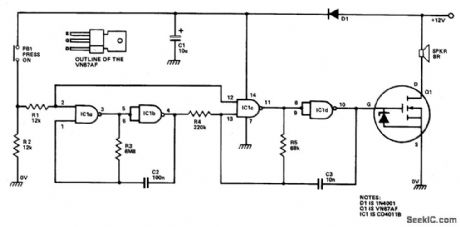
IC1a and IC1b are wired as a slow astable multivibrator and IC1c-IC1d are wired as a fast astable. Both are gated types, which can be turned on and off via PB1. The output of the slow astable modulates the frequency of the fast astable, and the output of the fast astable is fed to the external speaker via the Q1 VMOS power FET amplifier stage. (View)
View full Circuit Diagram | Comments | Reading(745)
SIREN_ALARM_SIMULATES_STAR_TREK_RED_ALERT
Published:2009/7/6 5:43:00 Author:May

The signal starts at a low frequency, rises for about 1.15 seconds to a high frequency, ceases for about 0.35 seconds, then starts rising again from a low frequency, and so on ad infinitum. (View)
View full Circuit Diagram | Comments | Reading(1450)
ELECTRONIC_SHIP_SIREN
Published:2009/7/6 5:40:00 Author:May
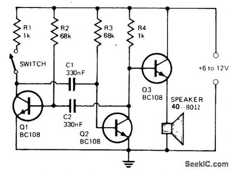
The circuit consists of a multivibrator (Q1 & Q2), and a low power output stage Q3. The speaker should have an impedance in the region of 40 to 80 ohms. To use a low impedance speaker, connect an output transformer from the emitter of Q3 to ground. C1 and C2 determine the pitch of the siren and the values specified will provide a tone of about 300 Hz.Quiescent current is negligible. The output at the collector of Q2 can also be fed into an amplifier input via a 1 pF electrolytic, in series with a 12 k resistor.
(View)
View full Circuit Diagram | Comments | Reading(802)
SIREN_USES_TTL_GATES
Published:2009/7/6 5:40:00 Author:May

The siren consists of two oscillators which generate the tones. A third oscillator is used to switch the others on and off alternately, giving the two-tone effect. By changing the capacitor values different tones can be produced. (View)
View full Circuit Diagram | Comments | Reading(456)
TOY_SIREN
Published:2009/7/6 5:38:00 Author:May
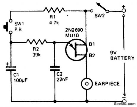
This circuit can be built small enough to fit inside a toy. The circuit consists of a relaxation oscillator utilizing one unijunction transistor (2N2646, MU10, 71543). R2 and C2 determine the frequency of the tone. Pushing the button, SW1 charges up the capacitor and the potential at the junction of R2 and C2 rises, causing an upswing in the frequency of oscillation. On releasing the pushbutton the charge on C2 will drop slowly with a proportional reduction in the frequency of oscillation. Manual operation of the button at intervals of approximately 2 seconds will produce a siren sound. (View)
View full Circuit Diagram | Comments | Reading(2360)
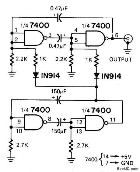
7400_SIREN
Published:2009/7/6 5:37:00 Author:May

Two NAND gates are used for the oscillator, and two as the control. If the two-tone speed needs to be altered, the 220 μF capacitors can be changed (larger for slower operation). If the frequency of the oscillator is to be changed, the 0.2 and 0.1 μF capacitors can be varied and the value of R1 can be increased. To change frequency range between the two notes, alter the 1.5 k (1.500) resistor. (View)
View full Circuit Diagram | Comments | Reading(824)
GLITCH_FREE_TURBO_CIRCUIT
Published:2009/7/6 5:36:00 Author:May
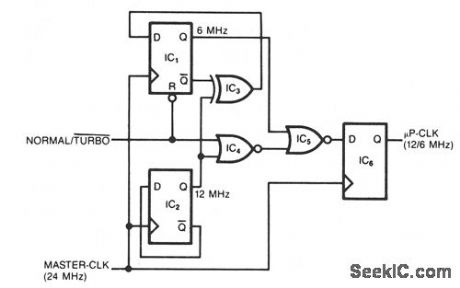
This simple circuit generates a dual-speed clock for personal computers. The circuit synchronizes your asynchronous switch inputs with the master clock to provide glitch-free transitions from one clock speed to the other. The dual-speed clock allows some programs to run at the higher clock speed in order to execute more quickly. Other programs-for example, programs that use loops for timing-can still run at the lower speed as necessary. The circuit will work with any master-clock. frequency that meets the flip-flops' minimumpulse-width specs.
The two D two flip-flops, IC1 and IC2, and an XOR gate, IC3, form a binary divider that develops the 6- and 12-MHz clocks. When the NT signal is low, the reset pin forces the 6-MHz output low. On the other hand, when the NT signal is high, IC3 blocks the 12-MHz output. Therefore, only one of the two clock signals passes through IC3 and gets clocked into IC6. Because the master-clk signal clocks IC6, asynchronous switching of the NT signal can't generate an output pulse shorter than 41 μs (1/24 MHz). Also, the synchronization eliminates glitches. (View)
View full Circuit Diagram | Comments | Reading(528)
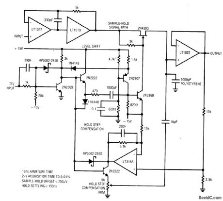
HIGH_PERFORMANCE_SAMPLE_AND_HOLD
Published:2009/7/6 5:36:00 Author:May
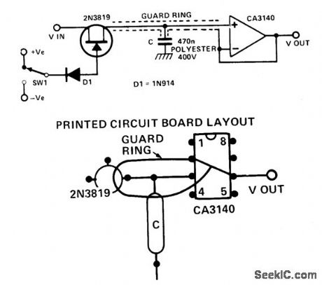
Circuit Notes
When switch SW1 is positive, the FET is turned on, and has a resistance of about 400 ohm. The input voltage charges up the capacitor through the FET. When SW1 is negative, the FET is turned off (pinched off). To get a long storage time, the op amp mus, have a very low input bias current. For the CA3140, this current is about 10 pico amps. The rate at which the capacitor will be discharged by this current is based on the equation, C (dv/dt)=i where dv/dt is the rate of change of voltage on the capacitor.Therefore: (View)
View full Circuit Diagram | Comments | Reading(550)
THREE_PHASE_CLOCK_FROM_AREFERENCE_CLOCK
Published:2009/7/6 5:35:00 Author:May
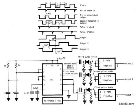
The circuit provides three square wave outputs with 120' of phase difference between each other. Reference clock frequency is twice that of the required frequency. This can be obtained from a crystal oscillator with a chain of dividers or by using LM555 in 50% duty cycle astable mode. If1/T is the frequency of the reference clock, the dual timer 556 is connected to give two mono-stable output pulses of duration T/3 and 2T/3. The first timer R and C value are adjusted so that ta 1.1RaCa = T/3 and the second timer R and C values so that tb = 1.1RbCb =2T/3. For triggering the two monostables a negative pulse train (1st) is derived from the reference clock with a differentiator and a clipper combination as shown. The three pulse trains trigger three JK flip flops giving three phase square wave outputs. (View)
View full Circuit Diagram | Comments | Reading(1247)
LOW_POWER_ACTIVE_FILTER_WITH_DIGITALLY_SELECTABLE_CENTER_FREQUENCY
Published:2009/7/6 5:34:00 Author:May

The switchable center frequency active filter allows a decade change in center frequency. (View)
View full Circuit Diagram | Comments | Reading(674)
MULTIFUNCTION_SIREN_SYSTEM
Published:2009/7/6 5:32:00 Author:May

The circuit uses a CA3130 BiMOS op amp as a multivibrator to control the siren's rate. A CA3094 used as a VCO is followed by a CA3082 transistor array used to drive a speaker. A Manual or Auto mode switch allows the user to select either intermittent or continuous siren operation, respectively. In addition, three switches are available that control Mode , Attack , and Rate .
(View)
View full Circuit Diagram | Comments | Reading(1497)
ELECTRONIC_CROWBAR
Published:2009/7/6 5:31:00 Author:May
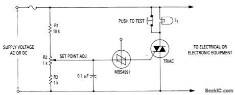
Where it is desirable to shut down equipment rather than allow it to operate on excessive supply voltage, an electronic crowbar circuit can be employed to quickly place a short-circuit across the power lines, thereby dropping the voltage across the protected device to near zero and blowing a fuse. Since the TRIAC and SBS are both bilateral devices, the circuit is equally useful on ac or dc supply lines. With the values shown for R1, R2 and R3, the crowbar operating point can be adjusted over the range of 60 to 120 volts dc or 42 to 84 volts ac. The resistor values can be changed to cover a different range of supply voltages. The voltage rating of the TRIAC must be greater than the highest operating point as set by R2. I1 is a low power incandescent lamp with a voltage rating equal to the supply voltage. It may be used to check the set point and operation of the unit by opening the test switch and adjusting the input or set point to fire the SBS. (View)
View full Circuit Diagram | Comments | Reading(1625)
6800_polled_interface_for_A_D_converter
Published:2009/7/23 21:07:00 Author:Jessie
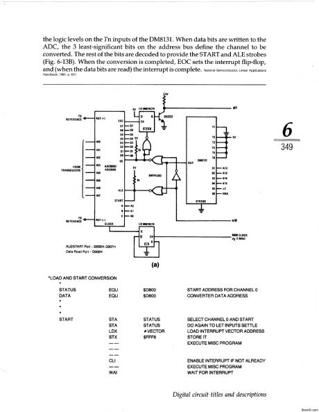


This circuit shows a 6800 polled I/O interface for the ADC0808/0809, with full address decoding. Figure 6-26B shows typical polled routines. (View)
View full Circuit Diagram | Comments | Reading(1176)
FAST,PRECISION_SAMPLE_HOLD
Published:2009/7/6 5:30:00 Author:May
View full Circuit Diagram | Comments | Reading(516)
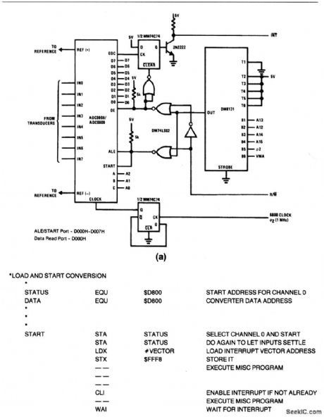
Port_address_structure_to_where_channel_is_a_separate_address
Published:2009/7/23 20:48:00 Author:Jessie
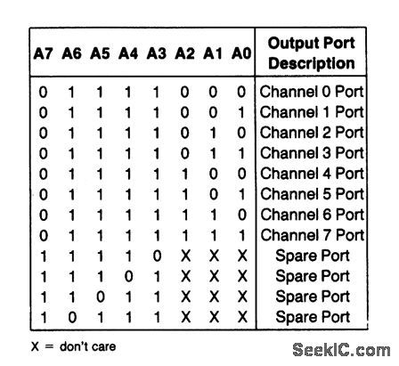

With this configuration, each channel of the ADC (Fig.6-20) looks like the same address. (View)
View full Circuit Diagram | Comments | Reading(556)
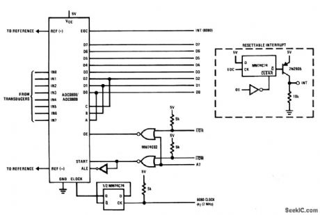
Port_address_structure_where_channel_is_selected_by_3_bit_word
Published:2009/7/23 20:47:00 Author:Jessie
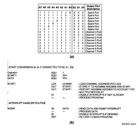


With this configuration, the ADC (Fig.6-20) looks like a port address where the channel is selected by the 3-bit status word written on the data bus. Figure 6-21 B shows a typical interrupt I/O routine. (View)
View full Circuit Diagram | Comments | Reading(510)
BIQUAD_AUDIO_FILTER
Published:2009/7/6 5:30:00 Author:May

This universal ftlter offers low-pass, high-pass, bandpass, band elimination, and all-pass functions.The Biquad consists of two successive integration stages followed by an inverting stage. The entire group has a feedback loop from the front to the back consisting of R1 which is chiefly responsible for controlling the center frequency, ωo. The first stage of integration is a poor integrator because R2 limits the range of integration. R2 and C form the time constant of the first stage integrator with R3 influencing gain H almost directly. The band-pass function is taken after the ftrst stage with the lowpass function taken after the third stage. The remaining ftlter operations are generated by various combinations of three stages.
The Biquad is orthogonally tuned, meaning that ωo. Q. and gain H can all be independently adjusted. The component values known will allow ωo, to range from 40 Hz to 20 kHz. The other component values give an adequate range of operation to allow for virtually universal filtering in the audio region. ωo Q. and gain H can all be independently adjusted by tuning R1 through R3 in succession. (View)
View full Circuit Diagram | Comments | Reading(882)
| Pages:260/471 At 20241242243244245246247248249250251252253254255256257258259260Under 20 |
Circuit Categories
power supply circuit
Amplifier Circuit
Basic Circuit
LED and Light Circuit
Sensor Circuit
Signal Processing
Electrical Equipment Circuit
Control Circuit
Remote Control Circuit
A/D-D/A Converter Circuit
Audio Circuit
Measuring and Test Circuit
Communication Circuit
Computer-Related Circuit
555 Circuit
Automotive Circuit
Repairing Circuit