
Basic Circuit
Index 243
64_CHANNEL_TWO_LEVEL
Published:2009/7/7 20:15:00 Author:May
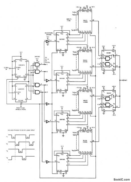
Two-level multiplexing system increases effective switching speeds when transmitting 64 analog signals on single transmission line. Four clock phases are generated with DM7473 2-bit counter that toggles on high-to-low dock edge. DM7400 NAND gates decode flip-flop outputs into required four clock phases. As clock phase goes from low tohigh state, DGt181 analog switch fed by it turns off and corresponding DM7493 4-bit binary counter is triggered to next address state for sampling of that input channel at output. Reset is used to set system for starting on first channel when power is applied.- Analog Switches and Their Applications, Siliconix, Santa Clara, CA, 1976, p 7-11-7-13. (View)
View full Circuit Diagram | Comments | Reading(811)
BFO_MULTIPLEXER
Published:2009/7/7 20:10:00 Author:May

Signal 455-kHz multi-mode detection system using RCA CD4001AE quad NOR gate functions as upper-sideband or lower-sideband crystal oscillator, tunable BF0 for CW, or limiter of IF signal for FM or synchronous AM reception, Desired oscillator or limiter is gated on by grounding its digital control line with S1A. Multimode reception occurs when multiplexed output of oscillators and limiter is applied to product detector-J. Regula, BFO Multiplexor for a Multimode Detector, Ham Radio, Oct. 1975, p 52-55. (View)
View full Circuit Diagram | Comments | Reading(750)
COMMUTATING_BANDPASS_FILTER
Published:2009/7/7 20:04:00 Author:May

CD4051 analog multiplexer serves for commutation and switching of eight low-pass filter sections. Multiplexer is driven by CD4024 binary counter that is clocked at 8 times desired 100-kHz center frequency Can be tuned by varying commutating frequency.J Tracy, CMOS Offers New Aρproach to Commutating Filters. EDN Magazine, Feb,5,1974.ρ94-95.
(View)
View full Circuit Diagram | Comments | Reading(4153)
1_kHz_COMB_FILTER
Published:2009/7/7 19:58:00 Author:May

DG508 eight-channel CMOS multiplexer is used in comb filter having fundamental frequency of 1 kHz. Sampling action provides response at each harmonic multiple except at 8 and 16 kHz (no response at Nf0 or 2Nf0). Used in selective filtering of periodic signals from background of nonperiodic noise interference, 7493 TTL binary counter provides necessary 3-bit binary count sequence from 8-kHz clock. Q is 50.- Analog Switches and Their Applications, Siliconix, Santa Clara, CA, 1976, p 5-17-5-18. (View)
View full Circuit Diagram | Comments | Reading(1808)
8_W_FLUORESCENT_LAMP_INVERTER
Published:2009/7/7 9:56:00 Author:May

This circuit has been designed to drive an 8-W fluorescent lamp from a 12-V source using an inexpen-sive inverter based on the ZTX652 transistor. The inverter will operate from supplies in the range of 10 to 16.5 V, thus making it suitable for use in on-charge systems such as caravanettes as well as periodically charged systems, such as camping lights, outhouse lights, etc. Other features of the inverter are an inaudi-ble 20-kHz oscillator and reverse polarity protection. (View)
View full Circuit Diagram | Comments | Reading(1117)
LINE_VOLTAGE_OPERATED_AUTOMATIC_NIGHT_LIGHT
Published:2009/7/7 9:55:00 Author:May
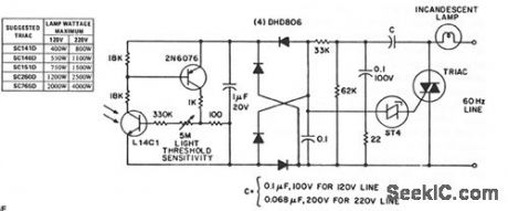
This circuit has stable threshold characteristics from its dependence on the photo diode current in the L14C1 to generate a base emitter voltage drop across the sensitivity setting resistor. The double phase shift network supplying voltage to the ST-4 trigger insures triac triggering at line voltage phase angles small enough to minimize RFI problems with a lamp load. This eliminates the need for a large, expensive inductor, contains the dV/dt snubber network, and utilizes lower voltage capacitors than the snubber ofrfi suppression network normally used. The addition of a programmable unijunction timer can modify this circuit to turn the lamp on for a fixed time interval each time its environment gets dark. Only the additions to the previous circuit are shown in the interest of simplicity. When power is applied to the lamp, the 2N6028 timer starts. Upon completion of the time interval, the H11C3 is triggered and turns off the lamp by preventing the ST-4 from triggering the triac. The SCR of the H11C3 will stay on until the L14C1 is illuminated and allows the 2N6076 to commutate it off. Because of capacitor leakage currents, tempera-ture variations and component tolerances, the time delay may vary considerably from nominal values. (View)
View full Circuit Diagram | Comments | Reading(685)
SOLID_STATE_LIGHT_DISSOLVER
Published:2009/7/7 9:51:00 Author:May
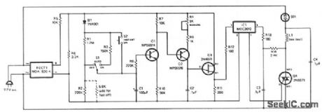
The dinuning action is controlled by varying the amount of current passed through triac Q4 and, thus, the lamp plugged into ac receptacle SOl. Unijunction transistor Q3 operates as a relaxation oscillator whose output pulse frequency depends on how fast capacitor C2 recharges after firing. Transistors Q1 and Q2 furnish the charging current, with the R3/C1 and RI/R2/C1 time-constant networks controlling the turn-on and turn-off times. Inside IC1 is a LED, a detector, and a small triac. In circuit, the low-level pulses coming from Q3 make the LED in IC1 emit short bursts of light that are picked up and converted into electrical current pulses by the internal detector. This small current triggers the internal triac, which then outputs the pulses to the gate of power triac Q4, triggering it on so that it delivers current to the lamp. Potentiometer R4 serves as a master control of the pulse rate and provides both manual control and a limit in the brightness of the lamp plugged into SO1. Momentarily pressing 52 causes the lamp to instantly turn on. Choke L1 suppresses any spikes produced by the power triac and limits interference with AM radio reception. No safeguards against interference need to be made for FM and TV reception, since these media are immune to this type of noise. (View)
View full Circuit Diagram | Comments | Reading(532)
LAMP_LIFE_EXTENDER
Published:2009/7/7 9:46:00 Author:May
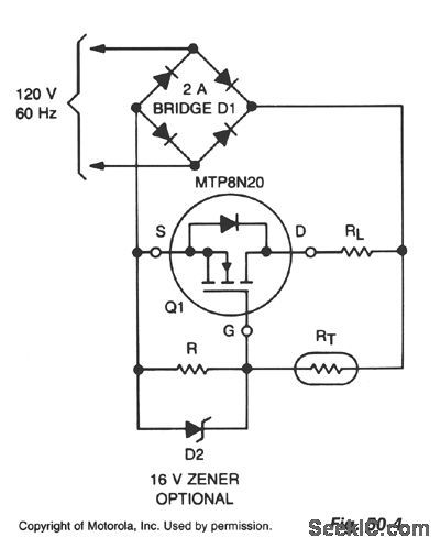
Lamp life can be extended by improving the conditions under which its filament is operated. This includes eliminating the inrush overcurrent surge and reducing the mechanical stress (vibration) on the filament caused by an ac source, The circuit shown controls the inrush current to the lamp without the 10 to 15 times-rated current stage that normally occurs when power is applied to a cold lamp. It does so by adjusting the inrush current over time to the inverse of the value normally experienced.RL is a standard tungsten lamp in the range of 15 to 250 W, R is 10-Ω and RT is a negative temperature coefflcient resistance that is initially 1.65 MΩ and decreases, by self-heating, to 150 KΩ in approximately 0.5 s. Use of the TMOS device allows high Ω values for R and RT, keeping drive power at a negligible level.This circuit has a number of advantages: very low power dissipation, long life, low-cost components, no significant effect on lamp ratings, negligible effect on efficiency, negligible RFI, and it can be used in hazardous environments. (View)
View full Circuit Diagram | Comments | Reading(598)
LIGHT_MODULATOR
Published:2009/7/7 9:44:00 Author:May
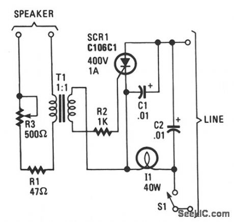
The lights seem to dance in time with the music. Line-voltage lamps of about 40 to 100 Mr do nicely. The current for the lamp is from an SCR. When low-level audio is present across T1, SCR1 is not triggered into conduction. A louder signal, how-ever, triggers the SCR so that the lamp lights and follows the sounds. Since SCR1 is operated by an alternating current, the rectifier moves out of the avalanche condition when the gate current is low. Potentiometer R3 lets you adjust the power reach-ing transformer T1, so that with normal operating volume, SCR1 triggers again and again, except dur-ing quiet passages. (View)
View full Circuit Diagram | Comments | Reading(609)
PSEUDORANDOM_SEQUENCER
Published:2009/7/7 9:43:00 Author:May
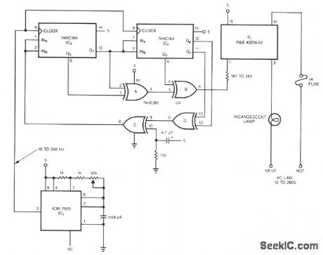
This pseudorandom sequencer drives a solid-state relay. If you power a low-wattage lamp from the relay, the lamp will appear to fiicker like a candle's flame in the wind; using higher-wattage lamps allows you to simulate the blaze of a fireplace or campfire. You can enhance the effect by using three or more such circuits to power an array of lamps.The circuit is comprised of an oscillator IC1 and a 15-stage, pseudorandom sequencer, IC2 through IC4. The sequencer produces a serial bit stream that repeats only every 32, 767 bits. Feedback from the sequencer's stages 14 and 15 go through IC4D and back to the serial input of IC2. Note the rc network feeding IC4C; the network feeds a positive pulse into the sequencer to ensure that it won't get stuck with all zeros at power-up. The leftover XOR gates IC4A and IC4B further scramble the pattern. The serial stream from IC4B drives a solid-state relay that features zero-voltage switching and can handle loads as high as 1 A at 12 to 280 Vac. (View)
View full Circuit Diagram | Comments | Reading(600)
HALOGEN_LAMP_DIMMER
Published:2009/7/7 9:41:00 Author:May
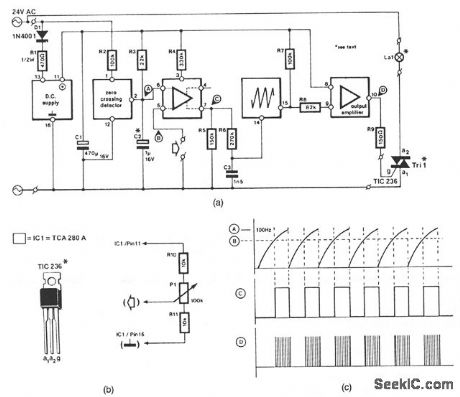
This circuit is suitable for fttting into slide projectors without a dimmer facility as with 24-Vac fed halo-gen lamps. With a few small alterations, it can also be used for dimming 12-V halogen lamps, but not those in a car, because these are fed from a dc source. The circuit shown in Fig. 50-1a is intended for operation from a 24-Vac supply, and can handle a lamp load of up to 150 W. For loads up to 250 W, the TIC236 should be replaced by a TIC246.Figure 50-1b shows detail of the connection of a potentiometer to the intensity control input of the TCA280A. Voltage divider R10-P1-R11 is fttted externally and can be fed from the stabilized voltage avail-able at pin 11 of IC1. The minimum and maximum intensities of the lamp are determined by R10 and R11, respectively. (View)
View full Circuit Diagram | Comments | Reading(2560)
POWER_INVERTER
Published:2009/7/7 9:39:00 Author:May

The transformer can be any 6.3 or 12.6 V type. Apply the 12-Vdc input so the positive goes to the transformer's center tap and the negative goes to the two transistor emitters. Any bridge-type rectifier and filter can be used at the output, if you need dc. (View)
View full Circuit Diagram | Comments | Reading(3662)
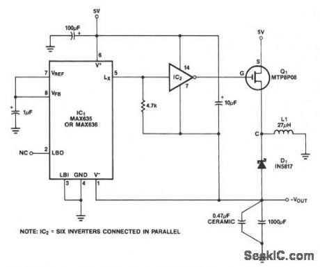
PRECISION_VOLTAGE_INVERTER
Published:2009/7/7 9:39:00 Author:May

This circuit allows a reference to be inverted with 1 ppm accuracy, features high input impe-dance, and requires no trimming. (View)
View full Circuit Diagram | Comments | Reading(1006)
COMPLEMENTARY_OUTPUT_VARIABLE_FREQUENCY_INVERTER
Published:2009/7/7 9:38:00 Author:May
U1 is a 4060 12-stage binary ripple counter that is used as a free-running oscillator; its frequency of oscillation is: 1/2.2 C1R2. The output of U1 is applied to U2, a 14-stage binary ripple counter that pro-vides square-wave outputs of 1/2, 1/4, 1/g, and 1/16 of the clock frequency. These signals are combined in U3 and U4 to provide a complementary drive for Q1 and Q2.Outputs from U3 and U4 are ac-coupled to Q1 and Q2 via C2 and C4, respectively. R3 and R4 adjust the gate drive to Q1 and Q2. Q1 and Q2 alternately draw current through opposing sides of the primary to synthesize an ac input voltage at a given frequency. Only one side of the primary of T2 is driven at one time, so maximum power output is half of the transformer rating. (View)
View full Circuit Diagram | Comments | Reading(964)
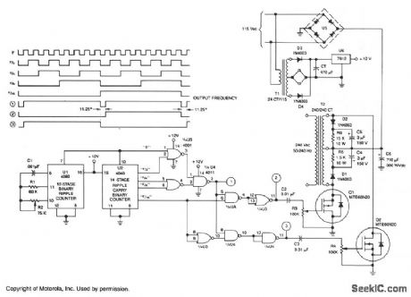
MEDIUM_POWER_INVERTER
Published:2009/7/7 9:36:00 Author:May
In this circuit, a CMOS inverter, such as the CD4069, is used to convert the open drain L, output to a signal suitable for driving the gate of an external P MOSFET The MTP8P03 has a gate threshold voltage of 2.0 V to 4.5 V, so it will have a relatively high resistance if driven with only 5 V of gate drive. To increase the gate drive voltage, and thereby increase efficiency and power handling capability, the negative supply pin of the CMOS inverter is connected to the negative output, rather than to ground. Once the circuit is started, the P MOSFET gate drive swings from + 5 V to - VOUT . At start up, the - VOUT is one Schottky diode drop above ground and the gate drive to the power MOSFET is slightly less than 5 V. The output should be only lightly loaded to ensure start up, since the output power capability of the circuit is very low until - VOUT is a couple of volts.This circuit generates complementary output signals from 50 to 240 Hz. Digital timing control ensures a separation of 10 to 15° between the fall time of one output and the rise time of the complementary out-put.The digital portion of inverter U1 to U4 controls the drive to Q1 and Q2, both MTE60N20 TMOS devices. These devices are turned on alternately with 11.25°separation between complementary out-puts. A +12-V supply for CMOS gates U1 to U4 is developed by T1, D3, D4, C7, and U6. The power supply for the TMOS frequency generator is derived from the diode bridge, U5, and capacitor C7; it is applied to the center tap of T2. (View)
View full Circuit Diagram | Comments | Reading(1016)
POWER_MOSFET_INVERTER
Published:2009/7/7 9:33:00 Author:May

This inverter can deliver high-voltage ac or dc, with a rectifier and filter, up to several hundred volts. The secondary and primary of T1-a 12.6 to 440 V power transformer, respectively-are reversed; e.g., the primary becomes the secondary and the secondary becomes the primary. Transistors Q1 and Q2 can be any power FET. Be sure to heat sink Q1 and Q2. Capacitors C1 and C2 are used as spike suppressors. (View)
View full Circuit Diagram | Comments | Reading(1947)
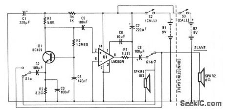
TWO_WAY_INTERCOM
Published:2009/7/7 9:29:00 Author:May
View full Circuit Diagram | Comments | Reading(779)
HANDS_OFF_INTERCOM
Published:2009/7/7 9:27:00 Author:May
Amplifier A increases the microphone's output to a usable level. The output signal is fed to op amp B, which inverts the signal 180°. A balance-control potentiometer connects across the outputs of amplifiers A and B. If an audio tone is fed into the microphone and the balance potentiometer's wiper is all the way over to the A output position, the tone will be heard at a high level. As the wiper is rotated toward the B output, the audio level will decrease until it just about disappears near the center of the potentiometer's range. As you continue to rotate the wiper, the signal will begin to increase once again.With the balance control set for a minimal output, the intercom's tendency to self-oscillate from acoustical feedback between the microphone and speaker is kept to a minimum. The microphone's ampli-fted signal at A's output is fed to the other intercom through the audio in/out cable. Since both intercom units are alike, the audio information coming from one unit feeds the other at the input of op amp B. The incoming audio is amplified slightly by op amp B and the output signal is sufficiently increased by the power amp to drive the speaker. (View)
View full Circuit Diagram | Comments | Reading(1097)
INTERCOM
Published:2009/7/7 9:25:00 Author:May
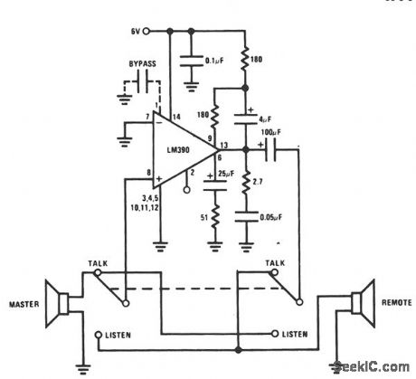
This intercom uses a single audio IC as a two-way amplifier, and the speakers as microphones. A single 6-V supply provides adequate audio volume. (View)
View full Circuit Diagram | Comments | Reading(0)
BIDIRECTIONAL_INTERCOM_SYSTEM
Published:2009/7/7 9:24:00 Author:May

This system uses μA759 audio IC devices and a common connection between the preamps as an inter-connect. Either mike can drive either speaker. Duplex operation is possible with only one cable (two wires). (View)
View full Circuit Diagram | Comments | Reading(828)
| Pages:243/471 At 20241242243244245246247248249250251252253254255256257258259260Under 20 |
Circuit Categories
power supply circuit
Amplifier Circuit
Basic Circuit
LED and Light Circuit
Sensor Circuit
Signal Processing
Electrical Equipment Circuit
Control Circuit
Remote Control Circuit
A/D-D/A Converter Circuit
Audio Circuit
Measuring and Test Circuit
Communication Circuit
Computer-Related Circuit
555 Circuit
Automotive Circuit
Repairing Circuit