
Basic Circuit
Index 255
PULSE_WIDTH_MULTIPLIER
Published:2009/7/6 9:37:00 Author:May
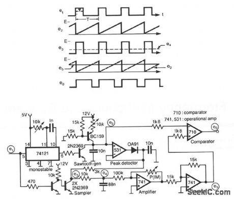
This circuit for multiplying the width of incoming pulses by a factor greater or less than unity is simple to build and has the feature that the multiplying factor can be selected by adjusting one potentiometer only. The multiplying factor is determined by setting the potentiometer in the feedback of the 741 amplifier. The input pulses e1, width T and repetition period T is used to trigger a sawtooth generator at its rising edges to produce the waveform e2 having a peak value of E volts. This peak value is then sampled by the input pulses to generate the pulse train e3 having an average value of e4(= ET/T) which is proportional to T and independent on T. The dc voltage e4 is amplified by a factork and compared with sawtooth waveform e2 giving output pulses of duration kT. The circuit is capable of operating over the frequency range 10 kHz- 100 kHz. Note that ic should be chosen less than T/T to ensure accurate pulse-width multiplication. (View)
View full Circuit Diagram | Comments | Reading(1018)
LIQUID_LEVEL_CHECKER
Published:2009/7/6 9:29:00 Author:May
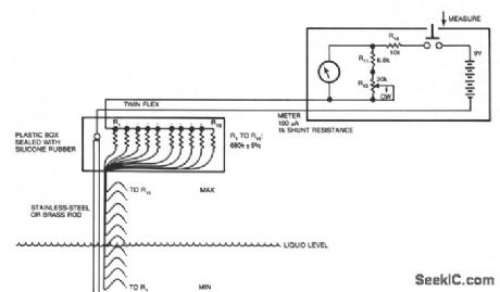
Although many circuits use the varying-capacitance method for checking liquid levels, this simple resistive circuit is much easier to construct. Even a tank of a liquid, such as water, has sufficient conduc-tive salts in solution for this method to work. The probe uses a metal rod that supports 10 insulated wires, which have stripped ends pointing down. As the level of liquid rises, resistors R1 through R10 are succes-sively brought into circuit, each drawing an extra 10 μA through the meter. Shunt resistors R11 and R13 calibrate the meter for a full-scale reading when the tank is full. Resistor R12 limits the current through the meter. If tank isn't rectangular-ie, if the volume of the liquid it contains isn't directly proportional to the liquid's depth-space the resistors accordingly or use a nonlinear progression of resistor values and retain constant resistor spacing. (View)
View full Circuit Diagram | Comments | Reading(590)
PCF8598 I2C Bus Control and Storage Integrated Circuit
Published:2011/7/29 0:13:00 Author:Michel | Keyword: Bus Control, Storage, Integrated Circuit

PCF8598 is I2C bus control and storage integrated circuit and it is widely used in KonKa WM series color TVs.
First,Functions Features
PCF8598 integrated circuit contains the I2C bus circuit, program control circuit, memory storage data circuit, the memory address processing circuit and some other auxiliary functions circuit.
Second,Pins Functions and Data
PCF8598 IC adopts 8 feet DIP package and its pins and functions on KonKa T2168K color TV are shown as table 1.
Table 1:PCF8598 IC Pins Functions and Data on KonKa T2168K Series Color TVs (View)
View full Circuit Diagram | Comments | Reading(623)
TONE_BURST_GENERATOR_FOR_EUROPEAN_REPEATERS
Published:2009/7/6 9:07:00 Author:May
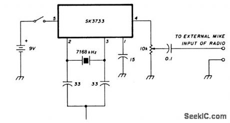
Most European repeaters must be brought up with a 1750-Hz tone. The SK3733 (also known as an ECG1197) IC contains a crystal oscillator and is divided by -256, 1024, 2048, and 4096. A 7168-kHz crystal is used; the divide-by-4096 output produces a 1750-Hz signal. (View)
View full Circuit Diagram | Comments | Reading(813)
CMOS_FLASHER
Published:2009/7/6 8:59:00 Author:May
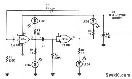
Uses a low cost CMOS IC to turn four LEDs on and off at a rate that is set by the values of R1, R2, C1, and C2. The pulse rate for the component values given for R1 and R2 is about one cycle every four seconds. By lowering the values of R1 and R2 to 220 KΩ, the pulse rate increases to 1 Hz. The LEDs flash in pairs, with LED1 and LED4 tuming together for one half of the time period, while LED2 and LED3 are on for the other half. The on/off duration of each pair of LEDs can be increased or decreased by changing the value of one of coupling capacitors C1 or C2. Increasing either capacitor's value by a factor of 10 will also increase the ON time of a pair of the LEDs for about the same factor. (View)
View full Circuit Diagram | Comments | Reading(576)
FIVE_LAMP_NEON_FLASHER
Published:2009/7/6 8:52:00 Author:May
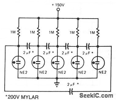
In this circuit, the number of lamps can be increased almost without limit. (View)
View full Circuit Diagram | Comments | Reading(479)
STRAIN_GAUGE_SIGNAL_CONDITIONER_WITH_BRIDGE_EXCITATION
Published:2009/7/6 8:51:00 Author:May
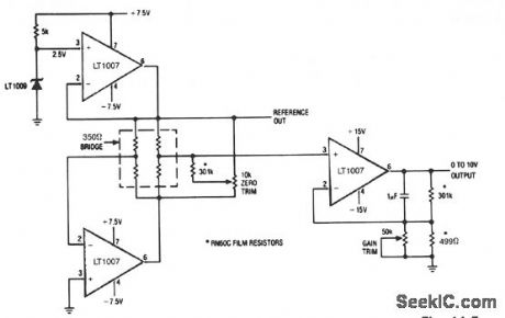
The LT1007 is capable of providing excitation current directly to bias the 350-Ω bridge at 5 V. With only 5 V across the bridge, as opposed to the usual 10 V, total power dissipation and bridge warm-up drift is reduced. The bridge output signal is halved, but the LT1007 can amplify the reduced signal accurately. (View)
View full Circuit Diagram | Comments | Reading(596)
SCR_FLASHER
Published:2009/7/6 8:48:00 Author:May
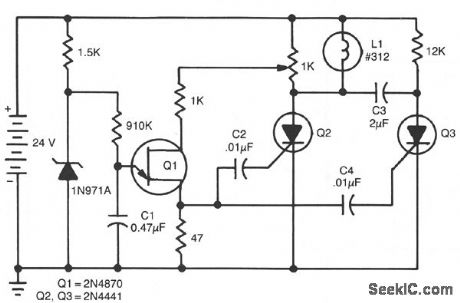
This dc flasher uses two SCRs and a unijunction oscillator clock to set the flash rate, which canbevaried by changing the value of C1. (View)
View full Circuit Diagram | Comments | Reading(790)
SCR_OHASER
Published:2009/7/6 8:47:00 Author:May
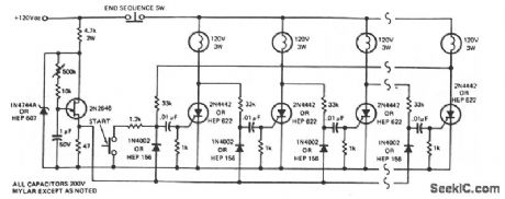
Each lamp lights in succession to give the appearance of a growing column. (View)
View full Circuit Diagram | Comments | Reading(483)
ACCURATE_NULL_VARIABLE_GAIN_CIRCUIT
Published:2009/7/6 8:46:00 Author:May
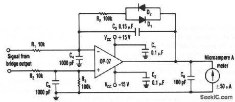
The circuit can use any general-purpose,low-offset,low-drift op amp,such as the OP-07.The differential signal from the bridge feeds an amplifier that drives an ordinary,rugged±50-μA meter. Near the null point,however, the drastically reduced signal level from the bridge requires very high gain to achieve a high null resolutio.To provide the variable-gain feature,the op amp's feedback path needs a dynamic resistance that increases as the input signal drops,Two common signal diodes,Dl and D2,in an antiparallel configuration in the feedback path supply function for all positive and negative inputs.To stabilize the opamp circuit at high gain,capacitors C3,C5,and C6 reduce response to high frequencies ;capacitors C1 andC2 bypass the amplifier's power supplies. (View)
View full Circuit Diagram | Comments | Reading(606)
AC_FLASHER
Published:2009/7/6 8:43:00 Author:May
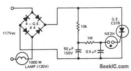
This ac line-operated flasher uses an SCR and is capable of flashing a large lamp. Flashing rate is determined by the 10-KΩ resistor and the 50-mF capacitor. Increasing or decreasing the value of the capacitor has a corresponding effect on the flash rate. (View)
View full Circuit Diagram | Comments | Reading(1317)
AUTO_ZEROING_SCALE
Published:2009/7/6 8:43:00 Author:May
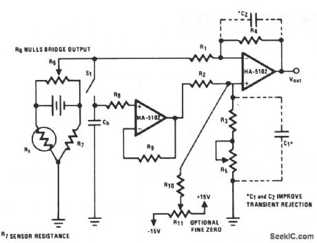
Electronic scales have come into wide use and the HA-510X, as a very low noise device, can improve such designs. This circuit uses a staingauge sensing element as part of a resistive Wienbridge. An auto-zero circuit is also incorporated into this design by including a sample-and-hold network.
The bridge signal drives the inverting input of a differentially configured HA-5102. The noninverting input is driven by the other half of the HA-5102 used as a buffer for the holding capacitor, CH. This second amplifier and its capacitor CH form the sampling circuit used for automatic output zeroing.The 20-KΩ resistor between the holding capacitor CH and the input terminal, reduces the drain from the bias currents. A second resistor RG is used in the feedback loop to balance the effect of R8. If R7 is approximately equal to the resistance of the strain gauge, the input signal from the bridge can be roughly nulled with R6. With very close matching of the ratio R4/R1 to R3/R2, the output offset can be nulled by closing S1. This will charge CH and provide a 0-V difference to the inputs of the second amplifier, which results in a 0-V output. In this manner, the output of the strain gauge can be indirectly zeroed. R10 and potentiometer R11 provide an additional mechanism for fine tuning VOUT, but they can also increase offset voltage away from the zero point. C1 and C2 reduce the circuit's susceptibility to noise and transients. (View)
View full Circuit Diagram | Comments | Reading(607)
ASTABLE_MULTIVIBRATOR
Published:2009/7/6 8:42:00 Author:May

The 4047 is configured as a free-running, asta-ble-multivibrator (oscillator) circuit. That configura-tion, offers three different outputs. The output pulses at theQ andQ output (pins 10 and 11, respectively) are the same as in the previous two circuits. The third output at pin 13 pulses twice as often as the outputs at 10 and 11. So, the circuit can be used to simultaneously provide both positive- and negative-trigger signals since theQ and Q output are never in the same state, and a clock frequency. Thus, the 4047 can replace both a simple oscillator (the 555, for instance) and a flip-flop in some applications. (View)
View full Circuit Diagram | Comments | Reading(0)
RUMBLE_FILTER_2
Published:2009/7/6 8:33:00 Author:May

View full Circuit Diagram | Comments | Reading(558)
FOURTH_ORDER_CHEBYSHEV_BANDPASS_FILTER
Published:2009/7/6 8:32:00 Author:May

View full Circuit Diagram | Comments | Reading(946)
FOURTH_ORDER_CHEBYSHEV_HIGH_PASS_FILTER
Published:2009/7/6 8:31:00 Author:May

View full Circuit Diagram | Comments | Reading(693)
SIXTH_ORDER_ELLIPTIC_HIGH_PASS_FILTER
Published:2009/7/6 8:30:00 Author:May

View full Circuit Diagram | Comments | Reading(676)
TYPICAL_ACTIVE_BANDPASS_FILTER
Published:2009/7/6 8:27:00 Author:May

View full Circuit Diagram | Comments | Reading(846)
STATE_VARIABLE_FILTER_WITH_MULTIPLE_FILTERING_OUTPUTS
Published:2009/7/6 8:26:00 Author:May

View full Circuit Diagram | Comments | Reading(663)
DYNAMIC_NOISE_FILTER
Published:2009/7/6 8:25:00 Author:May

View full Circuit Diagram | Comments | Reading(727)
| Pages:255/471 At 20241242243244245246247248249250251252253254255256257258259260Under 20 |
Circuit Categories
power supply circuit
Amplifier Circuit
Basic Circuit
LED and Light Circuit
Sensor Circuit
Signal Processing
Electrical Equipment Circuit
Control Circuit
Remote Control Circuit
A/D-D/A Converter Circuit
Audio Circuit
Measuring and Test Circuit
Communication Circuit
Computer-Related Circuit
555 Circuit
Automotive Circuit
Repairing Circuit