
Basic Circuit
Index 252
NONLINEAR_CUBIC_AND_QUADRATIC
Published:2009/7/6 22:04:00 Author:May

Provides four-quadrant operation with high accuracy over input amplitude range of several decades. Applications include analog computations for radar and ballistic problems,linearization of transducer characteristics, and teaching theory of quadratic equations. Article gives design equations and complete design produce.-H.Mcpherson,Non-Linear Function Generator,Wirelessworld,Oct.1972,p485-487. (View)
View full Circuit Diagram | Comments | Reading(719)
PULSE_RATIO_MODULATOR
Published:2009/7/6 22:01:00 Author:May

LM111 comparator serves with single transistor to provide pulse-train output whose average value is proportional to input voltage. Frequency of output is relatively constant but pulse width varies .Pulse-ratio accuracy is 0.1%. Circuit can be used to drive power stage of high-efficiency switching amplifier, or as pulse-width/pulse-height multiplier. Article tells how circuit works.-R.C. Dobkin, Comparators Can Do More than Just Compare, EDN Magazine, Nov. 1, 1972, p34-37. (View)
View full Circuit Diagram | Comments | Reading(848)
WIEN_BRIDGE_OSCILLATOR_USES_CMOS_CHIP
Published:2009/7/6 21:59:00 Author:May

View full Circuit Diagram | Comments | Reading(614)
1MHz
Published:2009/7/6 21:57:00 Author:May

Simple sinusoidal generator using Exar XR-22060 IC provides sine, triangle, or square outputs. For sine output, S1 is closed and RA and RB are adjusted tor minimum distortion. Exact output frequency f is 1/RC where R is about 2 megohms from pin 7 to ground and C is connected between pins 5 and 6. FM output is obtained when modulating input is applied to either pin 7 or 8. For AM output, modulation is applied to pin 1.-E. Noll, VHF/UHF Single-Frequency Conversion, Ham Radio, April 1975, p 62-67. (View)
View full Circuit Diagram | Comments | Reading(1045)
REDUC_DISTORTION_
Published:2009/7/6 21:54:00 Author:May

Use of UAF41 universal active filter at output of function generator reduces distortion of sine-wave output by eliminating some of harmonics. In typical application, two-pole active filter reduces 1% distortion down to 0.1%, using low-pass configuration. Articlegives design equations. For 1-kHz cutoff, R1, should be 159.2K.-Y. J. Wong, Design a Low Cost, Low-Distortion, Precision Sine-Wave Oscillator, EDN Magazine, Sept. 20, 1978,p107-113. (View)
View full Circuit Diagram | Comments | Reading(905)
MODIFIED_UJT_RELAXATION_OSCILLATOR_PRODUCES_GLEAN_AUDIO_SINUSOIDS
Published:2009/7/6 21:52:00 Author:May

Circuit NotesBy placing a tuned circuit in the UJT oscillator's current-pulse path, a 3750-Hz sinusoid can be created at B2 with the component values shown. (View)
View full Circuit Diagram | Comments | Reading(827)
AC_CONTROL_BY_TTL_I_O
Published:2009/7/6 21:35:00 Author:May
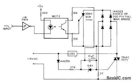
Output of. microprocessor drives LED of photocoupler through one section of 7414 hex Schmitt-trigger-input inverter. Output of phototransistor controls SCR connected across full-wave diode bridge. Current flow through bridge and SCR turns on triac, allowing alternating current to flow through load, Choose triac rated for handling required load current.-M. Boyd, Interfacing Tips, Kilo-baud, Feb. 1978, p 72-74. (View)
View full Circuit Diagram | Comments | Reading(1359)
PRECISION,LINEARIZED_PLATINUM_RTD_SIGNAL_CONDITIONER
Published:2009/7/6 21:34:00 Author:May

The circuit provides complete, linearized signal conditioning for a platinum RTD.This LTC1043 based circuit is considerably simpler than instrumentation or multi-amplifier based designs, and will operate form a single 5 V supply. A1 serves as a voltage-controlled ground referred current source by differentially sensing the voltage across the 998 phm feedback resistor. The LTC1043 section which does this presents a single-ended signal to A1's negative input, closing a loop. The 2 k 0.1 μF combination sets amplifier roll-off well below the LTC1043's switching frequency and the configuration is stable. Because A1's loop forces a fixed voltage across the 887 ohm resistor, the current through Rp is constant. A1's operating point is primarily fixed by the 2.5 V LT1009 voltage reference. (View)
View full Circuit Diagram | Comments | Reading(607)
DIGITAL_FOURIER
Published:2009/7/6 21:34:00 Author:May

Sine-wave generator produces Walsh-function approximation of sine function. Frequency of sine wave is set by square-wave input to pin 14 of 7493. Filter com ponents of opamp help smooth staircase wave form generated by summing Walsh-function components as weighted by resistors. Circuit is converter consisting of digital expander that expands input square wave into variety of digital waveforms and analog combiner that adds these waveforms to produce periodic analog output. Negative signs of Walsh harmonics are handled with digital inverter, and magnitudes are handled by choice of resistor value in summing junction. Signs and magnitudes are under microprocessor control. Net output is stairstep approximation to desired output, which can be smoothed by low-pass filter.-B. F. Jacoby, Walsh Functions: A Digital Fourier Series, BYTE, Sept. 1977, p 190-198. (View)
View full Circuit Diagram | Comments | Reading(2437)
VARIABLE_SQUARE_TRIANGLE_
Published:2009/7/6 21:30:00 Author:May

Dual pot R1-R3 varies frequency over range of 15-500 Hz when C1 is in circuit and 150-4800 Hz when C2 is in circuit. Each output has amplitude control.Opamps are Motorola MC3401P or National LM3900, and transistors are 2N2924 or equivalent NPN. Supply can be 12 VDC.-C. D. Rakes, Integrated Circuit Projects, Howard W. Sams, Indianapolis, IN, 1975, p 19-20. (View)
View full Circuit Diagram | Comments | Reading(562)
12_BITS_ON_8_BIT_BUS
Published:2009/7/6 21:28:00 Author:May

Arrangement shown speeds reading of 12 bits of data onto 8-bit microprocessor bus by simplifying checking procedure. Output of 74C107 flip-flop becomes DATA INVALID bit and is placed on bus during second read cycle. Simultaneously, circuit pulls 3 remaining bits (D4-D6) low through use of spare 8T97 gates. Article gives simplified 8080 subroutine required.-D. W. Taylor, Speed-Read 12 Bits onto an 8-Bit Bus, EDN Magazine, Sept. 5, 1978, p 70. (View)
View full Circuit Diagram | Comments | Reading(656)
SINE_WAVE_SHAPER
Published:2009/7/6 21:20:00 Author:May

Circuit Notes
Uses a CA3140 BiMOS op amp as voltage follower, together with diodes from a CA3019 array, to convert a triangular signal (such as obtained from a function generator) to a sine-wave output with typical THD less than 2%. (View)
View full Circuit Diagram | Comments | Reading(2000)
SQUARE_TO_SINE_WITH_PLL
Published:2009/7/6 21:19:00 Author:May

8038 Wavefrom generator simultaneously generates synthesized sine wave and square wave. Square-wave output closes phase-locked loop through 741 opamp IC2 and dual flip-flop IC1, while sine-wave output functions as converted output. Center frequency is 0.15/R9C3. R10 should be at least 10 times smaller than R9. If center frequency is 400 Hz, capture range is half that or ±100 Hz. When input is applied, phase comparator generates voltage related to frequency and phase difference of input and free-running signals, lC2 amplifies and offsets phase-difference signal. Sine output has less than 1% distortion, DC component of 0.5 Vcc, and minimum amplitude of 0.2 Vcc P-P.-L.S.Kasevich, PLL Converts Square Wave into Sine Wave, EDN Magazine, June 20, 1978, p 128. (View)
View full Circuit Diagram | Comments | Reading(2245)
05_Hz_TO_1_MHz_SINE_SQUARE_TRIANGLE_
Published:2009/7/6 21:10:00 Author:May

Uses Exar XR-2206 IC function generator in simple circuit that operates from dual supply ranging from ±6 V to ±12 V. Withl-μF capacitor for C, 2-megohm frequency control covers range of 0.5-1000 Hz. Range is 5-10,000 Hz with 0.1 μF, 50 Hz to 100 kHz with 0.01 μF, and 500 Hz to 1 MHz with 0.001 μF. Designed for experiments with active filters.-H. M. Berlin, Design of Active Filters, with Experiments, Howard W.Sams, Indianapolis, IN, 1977, p 9-10, (View)
View full Circuit Diagram | Comments | Reading(7854)
WIDE_FREQUENCY_TTL_CLOCK
Published:2009/7/6 21:06:00 Author:May

This free-running TTL square-wave oscillator has a variable frequency output over a 20:1 range or better through use of four of the six inverters in an SN7404 chip and the additional components shown.Frequency of oscillation is determined by the capacitor and the settings of potentiometers R2 and R4; the first pot controls width T1 and the second controls width T2 of the square-wave output. These adjustments are not completely independent. (View)
View full Circuit Diagram | Comments | Reading(790)
VOLTAGE_CONTROLLED_NONLINEAR
Published:2009/7/6 21:05:00 Author:May

Circuit produces function E0 = Xy/12, where X is input voltage in range of +10 mV to +10 V and Y is analog programming voltage in range of -0.4 V to -10 V. Uses Optical Electronics 2534 temperature-compensated log feedback elements, +5 V reference, two high-frequency opamps, and one low-frequency opamp. 2534 produces log conversion of input signal. 5898 multiplier serves to vary scale factor of log signal. With offsets used as shown, +10 V input will always produce +10 V output regardless of Y input. To set up, adjust R4 until output does not change with Y for +10 V input, then adiust R7 for +10 V output with +10 V input.- Voltage- Controlled Non-Linear Function Generator, Optical Electronics, Tucson, AZ, Application Tip 10263. (View)
View full Circuit Diagram | Comments | Reading(537)
SAMPLE_AND_HOLD_CIRCUIT_II
Published:2009/7/6 21:03:00 Author:May

Circuit Notes
This circuit rapidly charges capacitor Csto to a voltage equal to an input signal. The input signal is then electrically disconnected from the capacitor with the charge still remaining on Csto Since Csto is in the negative feedback loop of the operational amplifier, the output voltage of the amplifier is equal to the voltage across the capacitor.Ideally, the voltage across Csto should remain constant causing the output of the amplifier to remain constant as well. However, the voltage across Csto will decay at a rate proportional to the current being injected or taken out of the current summing node of the amplifier. This current can come from four sources: leakage resistance ofCsto, leakage current due to the solid state switch SW2, currents due to high resistance paths on the circuit fixture, and most important, bias current of the operational amplifier. If the ICH8500A operational amplifier is employed, this bias current is almost non-existent (less than 0.01pA). Note that the voltages on the source, drain and gate of switch SW2 are zero or near zero when the circuit is in the hold mode. Careful construction will eliminate stray resistance paths and capacitor resistance can be eliminated if a quality capacitor is selected. The net result is a low drift sample and hold circuit.The circuit can double as an integrator. In this application the input voltage is applied to the integrator input terminal. The time constant of the circuit is the product of R1 and Csto. (View)
View full Circuit Diagram | Comments | Reading(1507)
LOGGING_EXACT_TIME
Published:2009/7/6 21:01:00 Author:May

Used in microcomputer applications requiring recording of exact time of each event by data-logging printer,Uses555 timer and 7474 D flip-flop to produce interrupt request every 16.67 ms. Requires use of software routine that acknowledges interrupt, increments counter in known location to serve as time-of-day clock, and resumes interrupted program,Article diagrams software routine required. –Real-Time Software keeps Program Segments on Schedule, EDN Magazine. Novm,20.1976,p277-283. (View)
View full Circuit Diagram | Comments | Reading(492)
SIGLE_CONTROL_FOR_1000000;1_FREQUENCY_RANGE
Published:2009/7/6 21:00:00 Author:May

Uses two RCA CA313 opamps and CA3080A operational transconductance amplifier to generate square and triangle outputs that can be swept over range of o.1 Hz to 100 kHz with single 100K pot R1. Altemate voltage-control input is available for remote adiustment of sweep frequency. IC1 is operated as voltage-controlled current source whose output current is applied directly to integrating capacitor C1 in feedback loop of integrator IC2. R2 adiusts symmetry of triangle output. IC3 is used as controlled switch to set excursion limits of triangle output when square wave is desired.- Linear Integrated Circuits and MOS/FET's, RCA Solid State Division, Somerville, NJ, 1977, p 236-244 (View)
View full Circuit Diagram | Comments | Reading(561)
PCD3360_Ringer_With_PXE_Transducer_
Published:2009/7/6 20:57:00 Author:May

Two BST72 transistors provide an output voltage swing almost equal to the voltage at C3. Pins IS1 and IS2 are inoperative because DM = HIGH. Volume control is possible using resistor RV.
(View)
View full Circuit Diagram | Comments | Reading(1039)
| Pages:252/471 At 20241242243244245246247248249250251252253254255256257258259260Under 20 |
Circuit Categories
power supply circuit
Amplifier Circuit
Basic Circuit
LED and Light Circuit
Sensor Circuit
Signal Processing
Electrical Equipment Circuit
Control Circuit
Remote Control Circuit
A/D-D/A Converter Circuit
Audio Circuit
Measuring and Test Circuit
Communication Circuit
Computer-Related Circuit
555 Circuit
Automotive Circuit
Repairing Circuit