
Basic Circuit
Index 253
DIGITAL_CLOCK_WITH_ALARM
Published:2009/7/6 20:57:00 Author:May

View full Circuit Diagram | Comments | Reading(1818)
DC_CONTROL_BY_TTL_I_O
Published:2009/7/6 20:55:00 Author:May

Output of microprocessor drives LED of photocoupler through one section of 7414 hex Sch mitt-trigger-input inverter. Phototransistor switches power transistor or power Darlington on and off for control of direct current through load. With transistor having current gain of 30 and 20-mAcontrol cur-rent, load current can be 500 mA. With power Darlington having higher current gain, load can be several amperes. Since power de-vice is either off or saturated, heatsink can be small.-M. Boyd, Interfacing Tips, Kilobaud, Feb. 1978, p 72-74. (View)
View full Circuit Diagram | Comments | Reading(815)
CURRENT_CONTROLLED_SQUARE_TRIANGLE_GENERATOR
Published:2009/7/6 20:55:00 Author:May

CA3080 oparnp is connected as current-controlled integrator of both polarities for use in current-controlled triangle oscillator.Frequency depends on values of C and opamp bias current and can be anywhere in audio range of 20 Hz to 20 kHz. Square-wave output is obtained by using LM301A opamp as Schmitt trigger.-S. Franco, Current-Controlled Triangular/Square-Wave Generator, EDN Magazine, Sept. 5, 1973, p 91. (View)
View full Circuit Diagram | Comments | Reading(1694)
PROGRAMMABLE_MULTI_TONE_TELEPHONE_RINGER
Published:2009/7/6 20:53:00 Author:May

View full Circuit Diagram | Comments | Reading(682)
POWER_LINE_MODEM
Published:2009/7/6 20:52:00 Author:May

In the 100-kHz application from left to right, the coupling network feeds into the receiver section on the bottom of the chip. (The external components are summarized later.) The receive data output is pulled up via RPULL=10 K Ω. A minimum current of 10 mA sets the voltage drop across RPULL. Another voltage supply, VLOGIC, is shown if the user wants to have the output sent at TTL levels. Across the top is the transmitter section; going from right to left, the oscillator network, the class AB output stage (note feedback resistor RFEEDBACK) and the drive section. The LC values on the oscillator network should match those on the bandpass filter in the receiver. The drive stage feeds into the coupling network and back into the receive section. This enables the on-chip collision detection with listen-while-talking capability. This effect can be canceled, although the transmitter will still be connected to the receiver. (View)
View full Circuit Diagram | Comments | Reading(958)
TV_AS_DISPLAY_TERMINAL
Published:2009/7/6 20:52:00 Author:May

Simple switch inserted in ordinary TV receiver serves for feeding video output of microprocessor directly into video amplifier of set, to give low-cost display terminal. TV must have transformer-type power supply. Excellent set for monitor use is 12-inch Hitachi model P-04, having Hitachi SX chassis. This set has very wide bandwidth, giving sharp display with line widths up to 80 characters.-G. Runyan, The Great TV to CRT Monitor Conversion, Kilobaud, July 1977, p 30-31 (View)
View full Circuit Diagram | Comments | Reading(552)
1000;1_FREQUENCY_SWEEP_
Published:2009/7/6 20:51:00 Author:May

Permits varying output frequency of function generator over wide trequency range by using pot to vary control voltage Vc. Network consisting of two transistors and two diodes replaces usual charging resistor of Miller integrator in function generator, and has output cunent varying exponentially with input voltage. Electronic switch using pair of transistors is controlled by Schmitt trigger of function generator, which connects +Vc and -Vc altemately to charging circuit. If frequency pot is mechanically connected to strip-chart recorder, Bode plots of audio equipment can be made over entire audio range.-P.D. Hiscocks, Function Generator Mod. for Wide Sweep Range, Wireless World, Aug. 1973, p 374. (View)
View full Circuit Diagram | Comments | Reading(626)
DIGITAL_CTCSS_OSCILLATOR
Published:2009/7/22 1:24:00 Author:Jessie

Uses two gates of CM0S quad NAND gate as 3.2-kHz oscillator, one gate as buffer, and one as amplifier serving in active bandpass filter. Requires only one precision capacitor, and uses ordinary carbon resistors in frequency-determining network. C1 must be polystyrene, polycarbonate, Teflon, or silver mica. IC2 divides oscillator frequency by binary multiple. Output is fed back to gate of IC, for convening square wave into sine wave by filtering out high-frequency harmonics. Provides continuous- tone-coded subaudible squelch (CTCSS) for amateur repeater system to protect input from interference on commonly shared channels, Voltage regulator can be replaced by zener. Use base-collector junction of 2N3638 or equivalent transistor as varactor in parallel with transmitter crystal of true FM transmitter, to modulate output frequency of crystal oscillator for CTCSS encoding.-D. Dauben, Miniature Solid State Tone Encoders to Replace Reeds, CQ, Dec, 1975, p 42-45 and 76. (View)
View full Circuit Diagram | Comments | Reading(527)
CONTROL_TONE_DECODER
Published:2009/7/22 1:33:00 Author:Jessie

Permits monitoring local VHF FM repeater for calls from friends without having to listen to chatter of others or to repeater noise. Operation is similar to that of Motorola paging units in which special tone is transmitted to disable squelch of receiver being called. Each friend has tone encoder for his transmitter, set at correct frequency for connecting loudspeaker so desired call can be heard. Red LED comes on to confirm that loud-speaker is connected. Audio from receiver loud-speaker is fed into pin 3 of NE567V PLL U1.When correct tone frequency is received, pin 8 drops from 4V to near 0V, turning off Q1 and turning on Q2. Q2 closes relay K1, to connect loudspeaker, and holds it on until RESET switch is operated. Q2 is Radio Shack 276-1059 or other small SCR. CR1 is 1N4735, and CR2 is red LED.-K. Wyatt, Private Call System for VHF FM, Ham Radio, Sept.1977, p 2-64. (View)
View full Circuit Diagram | Comments | Reading(2127)
SILENT_COR
Published:2009/7/22 1:31:00 Author:Jessie

Solid-state carrier-operated relay uses Q1 to sense DC level change from receiver squelch and forward-bias Q2, thus latching Q3 on. Q4 and Q5 prevent C1 from accumulating a charge. Q6 is then disabled as long as there is an incoming signal. Q2 feeds terminals 1 and 3 for switching transmitter on and starting timer that shuts of f transmitter after 3 min of use.Q6 is timer that holds transmitter on for short time after incoming carrier has dropped out (carrier tail). B2 adjusts tail length, usually 1,-2 s.-D. L. Moon, Solid-State Repeater Control, QST, Oct. 1974, p 19-21. (View)
View full Circuit Diagram | Comments | Reading(1955)
AF_SQUELCH
Published:2009/7/22 1:29:00 Author:Jessie

Simple audio squelch circuit suppresses all input signals below preset threshold.-Circuits, 73 Magazine, Holiday issue 1976, p 170. (View)
View full Circuit Diagram | Comments | Reading(1993)
Setting Timing Circuit of Power Supply Connection
Published:2011/7/26 0:54:00 Author:Michel | Keyword: Power Supply, Setting Timing Circuit

Picture 1 is setting timing circuit of power supply connection.When the power is connected,triggering PWL of ME555 feet 2 is below (1/3)Ucc and feet 3 outputs pulse during the time decided by R2 and C2.Then,+Ucc charges C2 via R2 and VD1 and charging voltage rises to +Ucc.Because of VD1 isolation function,R1 and C1 negative trigger the pulse.VD1 is fast charging diode when the power is off and it can keep the circuit working reliably when the circuit is off and turned on again and again in short time.NE55 outputs T high-level of pulse which is determined by R3 and C3,namely, T=R3C3.
Picture 1:Setting Timing Circuit of Power Supply Connection (View)
View full Circuit Diagram | Comments | Reading(739)
Monolithic Stereo Play Intergrted Circuit
Published:2011/7/20 2:06:00 Author:Michel | Keyword: Monolithic, Stereo, Play Intergrted Circuit


LA4570 is cassette specific integrated circuit produced by SANYO Company.LA4570 are used in domestic, domestic assembly or import the monoplayer and cassette player.
First,LA4570 Inside Circuit Block Diagram and Pins FunctionsLA4570 integrated block is double preamplifying double power amplifier devices, with low voltage power supply and wide range, high gain, low consumption and less external components etc.advantages.One LA4570 and few external device can constitute monoplayer and cassette player.Its intergrated block inside circuit block diagram and typical application circuit are shown as picture 1.The IC adopts 16 feet DIP or flat package structure. The IC pins functions and data are shown as table 1.
Table 1: LA4570 IC Pins Functions and DataLA4570 Typical Application Circuit LA4570 typical application circuit of intergrated block is shown as picture 1. (View)
View full Circuit Diagram | Comments | Reading(2033)
TLC2932 Phase Locked Loop Clock Generating Integrated Circuit
Published:2011/7/20 1:34:00 Author:Michel | Keyword: Phase Locked, Loop Clock, Generating Integrated Circuit


TLC2932 is FLL clock generating IC produced by TEXAS.TLC2932 is mostly used in the DLP projection TV, in order to provide the clock signal for processing
circuits.TLC2932 integrated circuit contains the analog vco and phase detection circuit.Its inside circuit block diagram of intergrated block is shown as picture 1-1.
Picture 1-1:Inside Circuit Block Diagram of TLC2932 Intergrated Block
TL2932 adopts 14 feet DIP package and its pins functions and data are shown as table 1-2.
Table 1-2:Pins Functions and Data ofTLC2932 IC
(View)
View full Circuit Diagram | Comments | Reading(1023)
I2C Bus Control Storage Integrated Circuit of PCF8582
Published:2011/7/28 22:40:00 Author:Michel | Keyword: I2C Bus, Storage Integrated Circuit

PCF8582 is the I2C bus control electrically erasable/programming read-only memory integrated circuits, which is widely used in big TV screens and other video, audio, air conditioner microcomputer control system.
First,Functions Features
PCF8582 integrated circuit contains erasable/programmable read-only memory case, the I2C bus control interface and address signals interface circuits, etc.
Second,Pins Functions and Data
PCF8582 integrated circuit adopts feet 8 DIP package and its pins functions and data are shown as the table 1.
Table 1 :PCF8582 Pins Functions and Data (View)
View full Circuit Diagram | Comments | Reading(774)
SPEAKERPHONE
Published:2009/7/6 20:48:00 Author:May
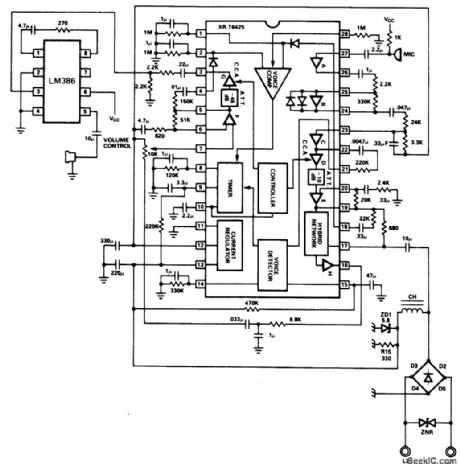
The XR-T6425 Speakerphone IC makes it possible to carry on conversation with-out using the handset, while the user is talking into a microphone and listening from a loudspeaker. It is ideal for hands-free conference calls. The XR-T6425 contains most of the circuits to eliminate singing and excessive background noise.
(View)
View full Circuit Diagram | Comments | Reading(2508)
POSITION_CONTROL_FOR_GRAPHICS
Published:2009/7/6 20:44:00 Author:May
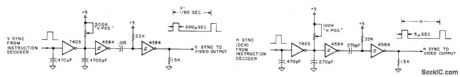
Six Inverters serve for moving entire character display to any position on TV screen,Display is produced by microprocessor through alphameric data-to-video converter. Circuit requires continuous feed of H and V signals from instruction decoder of microprocessor.-D. Lancaster, TVT Hardware Design, Kilobaud, Jan. 1978, p 64-68. (View)
View full Circuit Diagram | Comments | Reading(579)
TELEPHONE_IN_USEINDICATOR
Published:2009/7/6 20:42:00 Author:May
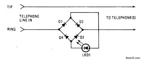
This circuit functions as a line-current sensor and can be connected in series with either of the phone lines. For the circuit to indicate an in use status for all phones on a single line, it must be connected in series with the phone line before, or ahead of all phones on the line. Since the power for the circuit is supplied by the phone company, a circuit could be added to each phone as an off-hook indicator. (View)
View full Circuit Diagram | Comments | Reading(513)
TELEPHONE_BLINKER
Published:2009/7/6 20:42:00 Author:May
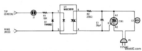
A small neon lamp is triggered into conduction by the telephone's ringing voltage, passes just enough current to activate the LED in optocoupler U1, which in tum triggers the 6-A Triac that controls I2-a 117-Vac lamp or bell. (Capacitor C1 is necessary only when the circuit is used to drive a bell.) The lamp will flash off-and-on at the ringing rate, which is normally around 20 Hz. If a 117 Vac bell is used, connect it in place of the lamp. (View)
View full Circuit Diagram | Comments | Reading(922)
A_D_converter_for_nonratiometric_transducer_inputs
Published:2009/7/23 0:56:00 Author:Jessie
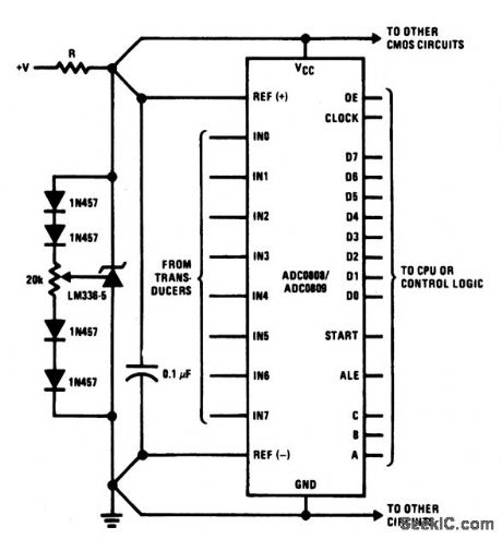
This circuit converts the output from 8 nonratiometric or absolute transducers to an 8-bit digital word using an ADC0808/0809, under control of a CPU or similar digital logic. The timing and internal functions shown in Fig. 6-13B and 6-13C also apply to this circuit. The LM336-5 acts as both a regulator and reference (for a 5-V or larger supply). Dropping resistor R is chosen so that, for the whole range of supply currents needed by the system (not just the ADC), the LM336-5 will stay in regulation. Again, use separate supply and reference traces to minimize noise. (View)
View full Circuit Diagram | Comments | Reading(481)
| Pages:253/471 At 20241242243244245246247248249250251252253254255256257258259260Under 20 |
Circuit Categories
power supply circuit
Amplifier Circuit
Basic Circuit
LED and Light Circuit
Sensor Circuit
Signal Processing
Electrical Equipment Circuit
Control Circuit
Remote Control Circuit
A/D-D/A Converter Circuit
Audio Circuit
Measuring and Test Circuit
Communication Circuit
Computer-Related Circuit
555 Circuit
Automotive Circuit
Repairing Circuit