
Basic Circuit
Index 251
DUTY_CYCLE_MODULATOR
Published:2009/7/6 22:56:00 Author:May

Uses half of LM339N or LM3302N quad comparator. With no modulation signal, output is symmetrical square wave generated by one of comparators. Constant-amplitude triangle wave is generated at inverting input of second comparator, and is relatively independent of supply voltage and frequency changes. Modulating signal varies switching points to produce duty-cycle modulated wave for such applications as class D amplification for servo and audio systems.-H. F. Stearns, Voltage Comparator Makes a Duty-Cycle Modulator, EDN Magazine, June 5, 1975, p76-77. (View)
View full Circuit Diagram | Comments | Reading(1050)
BALANCED_MODULATOR
Published:2009/7/6 22:51:00 Author:May
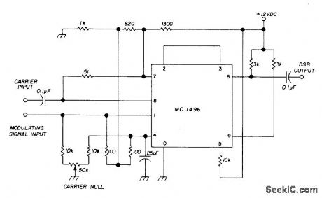
High-performance balanced modulator for 80-meter SSB transceiver uses Motorola MC1496IC,Adjust 50K pot for maximum carrier suppression of doublesideband output.-D, Hembling, Solid-State 80-Meter SSB Transceiver, Ham Radio, March1973,p6-17 (View)
View full Circuit Diagram | Comments | Reading(5029)
TRIANGLE_WAVE_CLIPPER
Published:2009/7/6 22:51:00 Author:May


Expression approximating sine function from 0 to 900is generated by function fitting and duplicated by using AD534L analog multiplier and appropriate close.tolerance (0.1%) resistors. Accuracy of sine wave is within ±0.5% at all points. Linearly increasing voltage of triangle develops rising sinusoidal output. Conversely, linearly decreasing input generates mirror of rising sinusoids. Increasing triangle waveform, then bringing it back to zero again, completes full cycle of sine-wave out-put.-R. Frantz, Analog Multipliers-New IC Versions Manipulate Real-World Phenomena with Ease, EDN Magazine, Sept. 5, 1977, p 125-129. (View)
View full Circuit Diagram | Comments | Reading(657)
SUPPRESSED_CARRIER_AM
Published:2009/7/6 22:46:00 Author:May

Double-balanced modulator using Signetics 511 transistor array gives output consisting of sum and difference frequencies of carrier and modulation inputs along with related harmonics. Circuit is self-balancing, eliminating need for pots, Output includes small amounts of carrier and modulating signal. Capacitor between emitters of Q3 and Q6 is selected to have low reactance at lowest modulating frequency.- Signetics Analog Data Manual, Signetics, Sunnyvale, CA, 1977, p 750-751. (View)
View full Circuit Diagram | Comments | Reading(780)
DRIVEN_CONSTANT_AMPLITUDE_SAWTOOTH
Published:2009/7/6 22:44:00 Author:May

Gives constant-amplitude output over input frequency range of 2-100 kHz. Input signal from SN74121 IC is 300-ns pulse that drives basic sawtooth generator Tr1-Tr2. Resulting sawtooth waveform is amplified by opamp A1 of MC3401P four-opamp package and fed to A2 which acts as comparator for amplitude-sensing, 25K threshold-setting pot is adjusted for maximum linearity of amplitude versus frequency, Rectangular-wave output ofA2 is filtered to give control voltage that is shifted in level by A3 and D1 to meet input voltage requirements of Tr2. Desired sawtooth output appears at source of Tr3.-J. N. Paine, Constant AmplitudeSawtooth Generator, Wireless World, 0ct.1975, p 473. (View)
View full Circuit Diagram | Comments | Reading(657)
DELTA_MODULATOR
Published:2009/7/6 22:43:00 Author:May

Uses LM111 comparator in basic pulse-ratio modulator circuit, with output pulse width and transition time fixed by external clock signal applied to gate of JFET switch a,. Average value of output is always proportional to input voltage,-R. C. Dobkin, Comparators Can Do More than Just Compare, EDN Magazine , Nov. 1, 1972, p 34-37. (View)
View full Circuit Diagram | Comments | Reading(1299)
20_20000_Hz_SQUARE_TRIANGLE
Published:2009/7/6 22:38:00 Author:May

Rt and Ct are chosen for upper frequency limit of 20 kHz,and oscillator is adjustable down to lower limit of 20 Hz with R5Circuit will operate up to 100 kHz if component values are suitably changed.A2should be offset-nulled by adjusting for best symmetry at lowest frequency. Total width of T of output waveform varies between 50 μs and 50 ms at frequency range covered.-W. G. Jung, IC Op-Amp Cookbook, Howard W. Sams, Indianapolis, IN, 1974, p 381-383. (View)
View full Circuit Diagram | Comments | Reading(648)
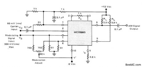
DSB_BALANCED_MODULATOR
Published:2009/7/6 22:33:00 Author:May

Provides excellent gain and carrier suppression by operating upper (carrier) differential amplifiers of Motorola MC1596G balanced modulator at saturated level and lower differential amplifier in linear mode. Recommended input levels are 60 m VRMS for carrier and 300 m VRMS maximum for modulating signal.-R. Hejhall, Input MC1596 Balanced Modulator, Motorola, Phoenix, AZ, 1975, AN-531, p 3. (View)
View full Circuit Diagram | Comments | Reading(621)
SINGLE_IC_AM
Published:2009/7/6 22:30:00 Author:May
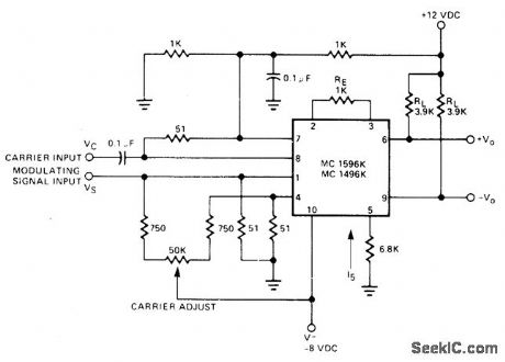
Adjustable carrier offset is added to carrier differential pairs to provide car-rier-frequency output that varies in amplitude with strength of modulation signal - Signetics Analog Data Manual, Signetics, Sunnyvale, CA, 1977, p 757. (View)
View full Circuit Diagram | Comments | Reading(610)
AMPLITUDE_MODULATOR
Published:2009/7/6 22:27:00 Author:May
Motorola type MC1596G balanced modulator functions as amplitude modulator when carrier null is unbalanced enough to insert proper amount of carrier into output signal. Provides excellent modulation from 0% to well over 100%.-R. Hejhall, MC1596 Balanced Modulator, Motorola, Phoenix, AZ, 1975, AN-531, p 7. (View)
View full Circuit Diagram | Comments | Reading(2074)
SUPPRESSED_CARRIER_MODULATOR
Published:2009/7/6 22:25:00 Author:May
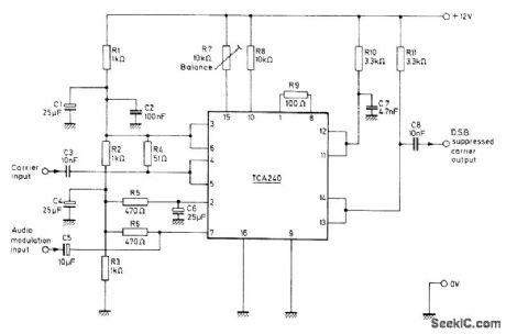
Mullard TCA240 dual balanced modulator-demodulator provides suppression of carrier frequency at output, as required for SSB or DSB operation of transmitter. Bias resistor R7 is adjusted for minimum carrier output to correct imbalance. Can be used as conventional AM modulator if biasing of circuit sections is deliberately unbalanced.- Applications of the TCA240, Mullard, London, 1975, Technical Note 18, TP1489. (View)
View full Circuit Diagram | Comments | Reading(1179)
DIODE_CANCELS_SUPPLY_CHANGES
Published:2009/7/6 22:22:00 Author:May

Adding any small-signal germanium diode to Intersil 8038 sine-square-triangle function generator as shown will compensate for changes in supply voltage. When using diode, change from 10 to 15 V produces only 5-Hz change in output over frequency range of 100-10,000 Hz. Technique can be applied to other IC function generators, such as Signetics 565, as well ast to 555 timers.-R. Liebman, Single Diode Compensates IC 0scillator, EDN Magazine, April 20, 1974, p 87. (View)
View full Circuit Diagram | Comments | Reading(724)
PULSE_HEIGHT_MODULATOR
Published:2009/7/6 22:21:00 Author:May

Used ahead of FET gate to reduce spike feedthrough. Voltage swing on FET gate is limited to difference between V1 and pinchoff voltage of FET. Zener D2 is matched to measured pinchoff voltage of FET in use.-M. D. Dabbs, Pulse Height Modulator, Wireless World, April1975, p 176. (View)
View full Circuit Diagram | Comments | Reading(545)
VOLTAGE_TO_PULSE_WIDTH
Published:2009/7/6 22:18:00 Author:May
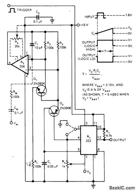
Constant-cur-rent source Q2 produces linear timing ramp across Ct in circuit of 322 IC timer A1, for comparison internally with 0-3.15 V applied to pin 7. Pulse is thus linearly variable function of control voltage Vc over dynamic range of more than 100:1. Circuit is highly flexible, permitting use of many other operational modes as covered in article. When AC waveform is applied to Vm, circuit operates as linear pulse-width modulator.-W. G. Jung, Take a Fresh Look at New IC Timer Applications, EDN Magazine, March 20, 1977, p 127-135. (View)
View full Circuit Diagram | Comments | Reading(0)
PULSE_DURATION_MODULATOR_USES_TIMER
Published:2009/7/6 22:14:00 Author:May
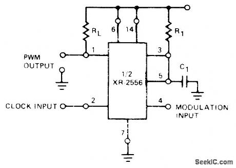
Half of Exar XR-2556 dual timer is connected to operate in monostable mode, for triggering with continuous pulse train. Output pulses are generated at same rate as input, with pulse duration determined by R1 and C1 Supply voltage is 4.5-16 V.- Timer Data Book, Exar Integrated Systems, Sunnyvale, CA, 1978, p 23-30. (View)
View full Circuit Diagram | Comments | Reading(1034)
THREE_WAVEFORM
Published:2009/7/6 22:12:00 Author:May
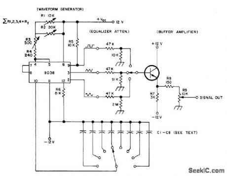
Gives simultaneous sine, square, and triangle outputs with low distortion (1%), high linearity (0.1%), 0.05 Hz to1 MHz frequency range, and duty cycle of 2% to 98%. Intersil 8038 waveform generator feeds buffer amplifier using 2N3709 transistor, switched to desired output waveform. Timing capacitors C1-C8, determining frequency decades of signal generator, start with 500,μF for 0.05 Hz to 0.5 Hz and decrease in submultiples of 10 to 500 pF for 50 kHz to 500 kHz. C8 is 250 pF for final range of 100 kHz to 1 MHz.-H. P.Fisher, Precision Waveform Generator, 73 Magazine, Dec. 1973, p 41-43. (View)
View full Circuit Diagram | Comments | Reading(2377)
LIGHT_BEAM_MODULATOR
Published:2009/7/6 22:11:00 Author:May
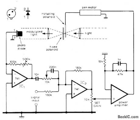
Intensity of light beam is modulated by rotating Polaroid vane driven by small motor. Since amplitude is not constant with change in frequency between 10 and 100 Hz, compensation is provided by sampling modulated beam with silicon photodiode that is linearized by IC1. Input and feedback signals are mixed by summing amplifier IC2, which drives noninverting power amplifier consisting of 741 opamp driving two OC28 power transistors connected in closed feedback loop having gain of 5. Power amplifier drives pen motor of modulator.-R. F. Cartwright, Constant Amplitude Light Modulator, Wireless World, Sept.1976, p 73. (View)
View full Circuit Diagram | Comments | Reading(571)
VEGATIVE_RAMP_
Published:2009/7/6 22:08:00 Author:May
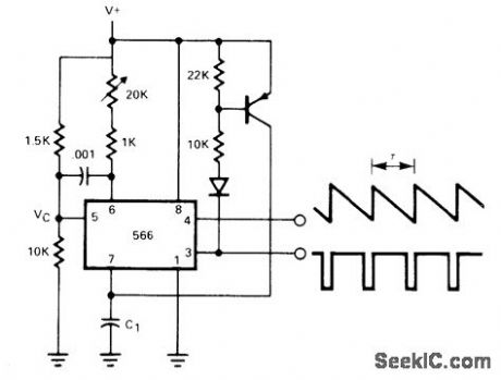
Connection shown for 566 function generator gives negative output ramp having period equal to 1/2f where f is normal free-running frequency of 566 as determined by supply voltage and RC values used. Ramp has very fast reset because PNP transistor charges timing capacitor C1 rapidly at end of discharge period. Short output pulse is available at pin 3.- Signetics Analog Data Manual, Signetics, Sunnyvale, CA, 1977, p 851. (View)
View full Circuit Diagram | Comments | Reading(1517)
DOUBLE_SIDEBAND_AM
Published:2009/7/6 22:07:00 Author:May
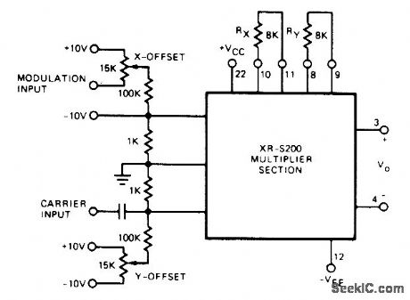
Connection shown for multiplier section of Exar XR-S200 PLL IC gives double-sideband AM output. X-offset adjustment for modulation input sets carrier out-put level, and Y-offset adiustment of carrier input controls symmetry of output waveform .Modulation input can also be used as linear automatic gain control (AGC)for controlling amplification with respect to carrier input signals, - Phase- Looked Loop Data Book, Exar Integrated Systems, Sunnyvale, CA, 1978, p9-16. (View)
View full Circuit Diagram | Comments | Reading(960)
SINGLE_SUPPLY_AM
Published:2009/7/6 22:04:00 Author:May

Motorola MC1545 gated video amplifier is connected as amplitude modulator operating from single supply. Artificial ground is established for IC at half of supply voltage by 5K resistors R1, which should draw much more than bias current of 15μA. All signals must be AC coupled to prevent application of excessive common-mode voltage to IC.- Gated Video Amplifier Applications-the MC1545, Motorola, Phoenix, AZ, 1976, AN-491, p 15. (View)
View full Circuit Diagram | Comments | Reading(586)
| Pages:251/471 At 20241242243244245246247248249250251252253254255256257258259260Under 20 |
Circuit Categories
power supply circuit
Amplifier Circuit
Basic Circuit
LED and Light Circuit
Sensor Circuit
Signal Processing
Electrical Equipment Circuit
Control Circuit
Remote Control Circuit
A/D-D/A Converter Circuit
Audio Circuit
Measuring and Test Circuit
Communication Circuit
Computer-Related Circuit
555 Circuit
Automotive Circuit
Repairing Circuit