
Basic Circuit
Index 242
WATER_LEAK_ISOLATOR
Published:2009/7/7 21:10:00 Author:May

Master indicator monitors large number of two-electrode waterleak detectors simultaneously, with each detector indicating presence of water by producing unique tone signal. Only two wires are needed between detectors and master indicator unit.Each detector location has quad NOR gate. First gate is water sensor, second is inverter, and last two form astable MVBR. When sensing electrodes are dry, resistance between them is above 500K and MVBR is disabled. When water drops resistance below 100K, MVBR oscillates at audio frequency determined by its RC time constant, equal to 1/1.4RC where R is in ohms and C is in farads. CP value in farads should be 1/1000 of lowest frequency used by detectors. L in henrys is about 1/600 of lowest frequency.-F. E. Hinkle, Multiplexed Detectors lsolate Water Leaks, Electronics, Dec. 11, 197S, p 116-117. (View)
View full Circuit Diagram | Comments | Reading(2427)
VISIBLE_RED_CONTINUOUS_LASER_GUN
Published:2009/7/7 21:09:00 Author:May


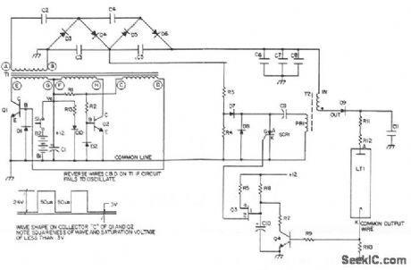
Q1 and Q2 switch the primary windings of transformer T1 via a square wave at a frequency determined by its magnetic properties. Diodes Dl and D2 provide base return paths for the feedback current of Q1 and Q2. The output winding of T1 is connected to a multiple section voltage multiplier. That multiplier consists of capacitors C1 through C5 and diodes D3 through D6. Resistors R3 and R4 divide the 800 V taken off at the junction of C3, and C5 for charging the dump capacitor C9 in the ignitor circuit. The ignitor, consisting of the T2 pulse transformer and capacitor discharge circuitry, provides the high-voltage dc pulse to ignite the laser the SCR1 dumping the energy of capacitor C9 into the primary of T2. The high-voltage pulses in capacitor C11 through rectifier diode D9. When C11 is charged to a LT1, ignition takes place and a current now flows that is sufficient to sustain itself at the lower voltage output of the voltage multiplier section. The path for this sustaining current is through the secondary of T2 and ballast resistors R11 and R12. The ignitor circuit is now deactivated by the clamping of Q3 emitter via Q4 being turned on by the voltage drop occurring across R10. This voltage drop will only occur when the laser tube is ignited and causes the SCR1 to cease firing; otherwise, the ignitor circuit would continue to operate, unnecessarily drawing on the limited power available.
(View)
View full Circuit Diagram | Comments | Reading(632)
RINGER_RELAY
Published:2009/7/7 21:06:00 Author:May
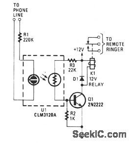
When the phone rings, the ring signal from the telephone company lights a neon lamp within a CLM3120 optocoupler. That causes a drop in the resistance of the CdS cell output of the device, turning on transistor Q1. When Q1 tums on, relay K1 is energized. The circuit should be connected in series with the lamp that is to be activated. (View)
View full Circuit Diagram | Comments | Reading(832)
SIX_GAME_VIDEO
Published:2009/7/7 21:05:00 Author:May
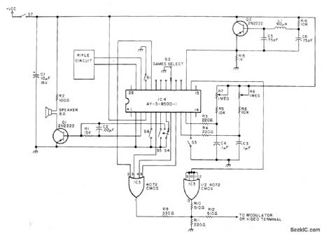

General Instruments AY-3-8500-1 MOS chip gives choice of hockey, squash, tennis, two types of rifle shoot, and practice games, all with sound effects and automatic scoring on 0-15 display at top of TV screen.Can be used with standard TV receiver (using RF modulator circuit) or with video monitor, S4 grounds base of Q1 when in manualserve mode, to eliminate steady boing when ball leaves playing field. R5-R8 position players on field.Article covers operation in detail and gives suitable rifle circuit. Supply is +6V. 2-MHz clock is at upper right.-A. Dorman, Six Games on a Chip, Kilobaud,Jan. 1977, p 130, 132, 134, 136, and 138. (View)
View full Circuit Diagram | Comments | Reading(3057)
ELECTRONIC_TELEPHONE_SET_WITH_REDIAL
Published:2009/7/7 21:03:00 Author:May

View full Circuit Diagram | Comments | Reading(814)
TWO_CHANNE_LOGIC_CONTROLLED
Published:2009/7/7 21:02:00 Author:May

Two CA3080A operational transconductance amplifiers are programmed on and off alternately by control logic, for multiplexing two inputs each up to ±5 V into single output. When control line E, is high or 1, input 1 appears at output; for logic 0, input 2 appears at output. Both channels operate at unity gain. Control logic is TTL-compatible.-W. G. Jung, IC Op-Amp Cookbook, Howard W. Sams, Indianapolis, IN, 1974, p 458-462. (View)
View full Circuit Diagram | Comments | Reading(596)
EIGHT_CHANNEL_MUX_DEMUX
Published:2009/7/7 20:58:00 Author:May
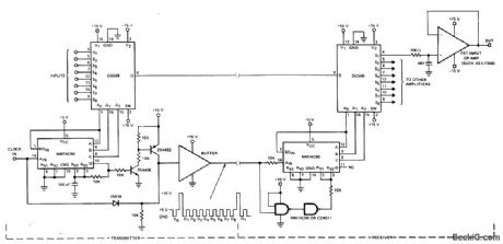
Provides for monitoring of all eight channels continuously at remote location instead of scanning channels at receiver, Each output of DG508 eight-channel analog multiplexor in receiver feeds its own opamp for driving readout. Similar DG508 at transmitter feeds inputs over single-wire line under control of MM74C90 presettable decade counter which also feeds pulse train over separate channel to receiver for timing and synchronization. 15-V reset pulse superimposed on 5-V clock pulses keeps channels synchronized.- Analog Switches and Their Applications, Siliconix, Santa Clara, CA, 1976,p 7-71-7-74. (View)
View full Circuit Diagram | Comments | Reading(887)
VHF_MODULATOR_
Published:2009/7/7 20:52:00 Author:May

Developed as interface between General Instruments AY-3-8500-1 TV game chip and antenna terminal of TV set. Adjust C1 to frequency of unused channel to which receiver is set for playing games. Article gives all circuits but covers construction only in general terms.-S. Ciarcia, Hey, Look What My Daddy Built!, 73 Magazine, Oct. 1976, p 104-108. (View)
View full Circuit Diagram | Comments | Reading(2702)
TELEPHONE_CONTROLLED_NIGHT_LIGHT
Published:2009/7/7 20:50:00 Author:May

When the telephone rings, or when the handset is lifted, the night light is turned on and remains on while the conversation takes place. When the handset is replaced in the cradle, the light remains on for about 11 s. During standby conditions, the -28 Vdc bias on the phone line maintains the output of U3 in a high state. When the ac ring signal is applied to the phone line, it is processed by the ring detector U1, producing a negative output pulse at pin 2 for each ring. These pulses trigger U2, causing its output to become high and the discharge transistor to turn off. The high output of U2 activates optoisolator U4, which turns on the night light. Each ring retriggers the timer and discharges C1, preventing it from reach-ing the 2/3 VDD threshold level. Thus, the night light will remain on while the phone is ringing and for about 11 s after the last ring. After 11 s, C1 will be charged to the U2 threshold level (2/3 VDD) resulting in the U2 output returning to a low level and its discharge output turning on, discharging C1. The lamp will turn off if the phone is not answered.
When the phone is answered, a 1-KΩ load is placed across the phone. This removes the differential input to op amp U3, causing its output to become low, and capacitor C1 starts discharging through R1. As long as the voltage across C1 remains low, timer U2 cannot start its cycle and the lamp will remain on. When the phone is hung up, the low impedance is removed from the phone line and the differential voltage across the line causes the U3 output to become high. This allows C1 to start charging, initiating the timing that will turn off the night light. (View)
View full Circuit Diagram | Comments | Reading(1013)
60_LED_HYPNOTIC_SPIRAL
Published:2009/7/7 20:50:00 Author:May

LEDs are mounted on display board in spiral arrangement and wired in matrix connected to ICs so each LED is lighted in sequence as IC1 and lC2 carry out counting function. IC3 is square-wave oscillator with frequency determined by C1 and setting of R2. Output pulses are used to clock lC1 to advance count, with carry output of IC1 clocking every tenth count. At end of 60 counts, both ICs reset to zero for new sequence. Inherent current limiting of ICs makes dropping resistors unnecessary for LEDs.-F. Blechman, Digitrance, Modern Electronics, Dec, 1978, p 29-31. (View)
View full Circuit Diagram | Comments | Reading(3473)
16_CHANNEL_SIMPLIFIED_SEQUENTIAL_MUL_TIPLEXING
Published:2009/7/7 20:46:00 Author:May

Two National LF13508 eight-channel multiplexors are connected so enable pins are used to disconnect one multiplexer while the other is sampling. Any number of eight-channel multiplexers can be connected in this way if speed is not prime system requirement.- FET Databook, National Semiconductor, Santa Clara, CA, 1977, p 5-79-5-81. (View)
View full Circuit Diagram | Comments | Reading(584)
SINGLE_CHIP_PULSE_TONE_DIALER
Published:2009/7/7 20:43:00 Author:May

The XR-75990 single-chip pulse/tone Dialer is a silicon gate CMOS circuit which performs both pulse and tone functions. It is designed to operate directly from the telephone line or on a separate small power supply. A 17-digit buffer is provided for redial feature. (View)
View full Circuit Diagram | Comments | Reading(1973)
HIGH_SPEED_16_CHANNEL
Published:2009/7/7 20:43:00 Author:May
Fast two-channel multiplexer using National AM182 dual analog switch provides second-level multiplexing by accepting outputs of each LF13508 eight-channel multiplexer and feeding these outputs sequentially into 8-bit successive-approximation A/D converter. Technique makes throughput rate of system independent of analog switch speed. With maximum clock frequency of 4.5MHz,throughput rate is 31.250 samples per second per channel- FET Databook, National Semiconductor, Santa Clara, CA, 1977, p 5-79-5-80. (View)
View full Circuit Diagram | Comments | Reading(896)
HOWLING_BOX
Published:2009/7/7 20:40:00 Author:May


Tone oscillator driving loudspeaker is sealed into wood or plastic box, with reed switch mounted on one face of box and pushbutton of other switch projecting out through hole in box. Place DO NOT TOUCH label on button. When button is pushed despite yvaming, SCR latches and applies power to AF oscillator. Only way to turn off howling is to hold large permanent magnet against location of reed switch, to oppose field of magnet glued on switch and make reed contacts open. If mercury swhch is used in box in place of pushbut-ton, alarm goes off when box is picked up.-P.Walton, Now What Have I Done?, 73 Magazine, May 1975, p 81. (View)
View full Circuit Diagram | Comments | Reading(597)
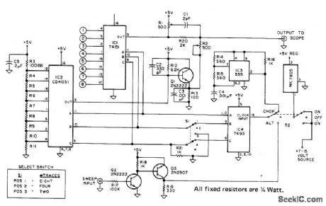
8_CHANNEL_CRO_MULTIPLEXER
Published:2009/7/7 20:37:00 Author:May

Simple adapter converts any single-trace oscilloscope into professional 8-channel model by multiplexing eight input signals into one output for vertical amplifier. Discrete voltages are picked off resistor divider chain sequentially and added to digital input signal so trace is shifted fast enough to produce eight individual traces. Addressing for 74151 digital multiplexer requires 3 bits of binary code to address all eight channels in sampling sequence. As each channel is sampled, its logic level (1 or 0) appears at pin 5 of 74151 for feed to vertical input of CRO. Developed for troubleshooting in digital circuits.-W. J. Prudhomme, Build an Eight Channel Multiplexer for Your Scope, Kilobaud, April 1977, p 29-32. (View)
View full Circuit Diagram | Comments | Reading(1754)
64_CHANNEL_TWO_LEVEL_HIGH_SPEED
Published:2009/7/7 20:33:00 Author:May
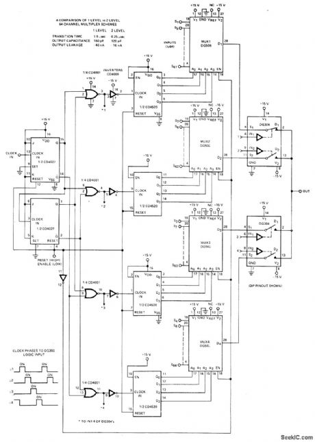
Foul DG506 16-channel multiplexers serve for first multiplexer level, and two DG304 high-speed dual analog switches serve in second level for switching DG506 outputs to single output of multiplexer. As one multiplexor is being sampled at output, other multiplexers are being switched to next address line; this shortens overall system transition time from 1.5μs to 0.25μs. Two-level system also lowers output node capacitance and output leakage. CMOS digital logic controls entire system.- Analog Switches and Their Applications, Siliconix, Santa Clara, CA, 1976, p 7.82-7-84. (View)
View full Circuit Diagram | Comments | Reading(589)
EXTENDED_PLAY_CIRCUIT
Published:2009/7/7 20:30:00 Author:May

A single op amp-one of four contained in the popular LM324-is operating in a variable pulsewidth, free-running squarewave oscillator circuit, with its timed output driving two transistors that control the on/ off cycle of the tape-drive motor.The oscillator's positive feedback path holds the secret to the successful operation of the variable on/ off timing signal. The two diodes and pulsewidth potentiometer R8 allows the setting of the on and off time, without affecting the oscillator's operating frequency. One diode allows only the discharge current to flow through it and the section of R8 that it's connected to. The other diode, and its portion of R8, sets the charge time for the timing capacitor, C3. Since the recorder's speed is controlled by the precise off/on timing of the oscillator, a simple voltage-regulator circuit (Q1, R3, and D4) is included.Connecting the speed control to most cassette recorders is a simple matter of digging into the recorder and disconnecting either of the motor's power leads, the ground or common side might be best, and connecting the recorder through a length of small, shielded cable to the control circuit. In some recorders, a remote input jack is furnished to remotely turn on and off the recorder. Before going in and modifying a recorder with a remote jack, try connecting the circuit to the external remote input. (View)
View full Circuit Diagram | Comments | Reading(1400)
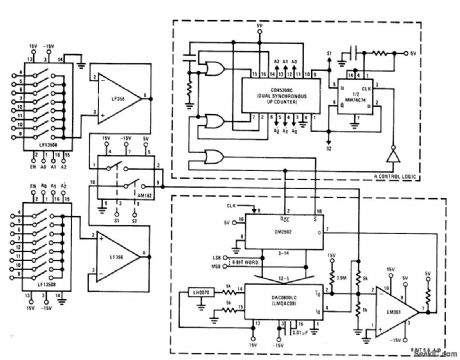
FOUR_CHANNEL_DIFFERENTIAL
Published:2009/7/7 20:28:00 Author:May
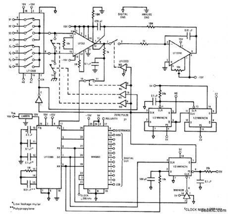
Low-speed high-accuracy data acquisition unit acquires analog input signal differentially with LF13509 IC and preconditions it through LF352 instrumentation amplifier having automatic zeroing circuit. Timing is provided by MM5863 12-bit A/D converter and lower MM74C74 flip-flop. Upper two flip-flops form 2-bit up counter for channel select. Instrumentation amplifier is zeroed at power-up and after each conversion. Maximum clock frequency depends on required accuracy and minimum zeroing time of instrumentation amplifier.- MOS/LSI Databook, National Semiconductor, Santa Clara, CA, 1977, p 5-2-5-22. (View)
View full Circuit Diagram | Comments | Reading(1073)
BATTERY_SPLITTER
Published:2009/7/7 20:23:00 Author:May
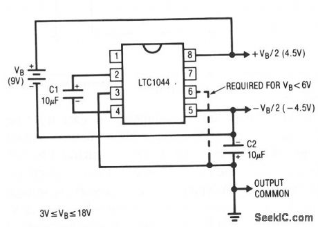
A common need in many systems is to obtain positive and negative supplies from a single battery. Where current requirements are small, the circuit shown is a simple solution. It provides symmetrical ±output voltages, both equal to one half the input voltage. The output voltages are referenced to pin 3, output common. If the input voltage between pin 8 and pin 5 exceeds 6 V, pin 6 should also be connected to pin 3, as shown by the dashed line.Higher current requirements are served by an LT1010 buffer. The splitter circuit can source or sink up to ±150 mA with only 5 mA quiescent current. The output capacitor, C2, can be made as large as necessary to absorb current transients. An input capacitor is also used on the buffer to avoid high frequency instability that can be caused by high source impedance. (View)
View full Circuit Diagram | Comments | Reading(476)
WIDEBAND_DIFFERENTIAL_INPUT
Published:2009/7/7 20:22:00 Author:May

Circuit design using PN4392 FET switches driven by 2N5457 general-purpose FETs allows handling of high-frequency signals at toggle rates up to 1 MHz for multiplexing to any desired number of channels,- FET Databook, Nation Semiconductor, Santa Clara,CA,1977,p 6-26-6-36. (View)
View full Circuit Diagram | Comments | Reading(521)
| Pages:242/471 At 20241242243244245246247248249250251252253254255256257258259260Under 20 |
Circuit Categories
power supply circuit
Amplifier Circuit
Basic Circuit
LED and Light Circuit
Sensor Circuit
Signal Processing
Electrical Equipment Circuit
Control Circuit
Remote Control Circuit
A/D-D/A Converter Circuit
Audio Circuit
Measuring and Test Circuit
Communication Circuit
Computer-Related Circuit
555 Circuit
Automotive Circuit
Repairing Circuit