
Basic Circuit
Index 256
SCRATCH_FILTER
Published:2009/7/6 8:23:00 Author:May

View full Circuit Diagram | Comments | Reading(0)
STATE_VARIABLE_ACTIVE_FILTER
Published:2009/7/6 8:22:00 Author:May

A generalized circuit diagram of the two-pole state-variable active filter is shown. The state-variable filter can be inverting or noninverting and can simultaneously provide three outputs: low-pass, bandpass, and high-pass. A notch filter can be realized by adding one summing op amp.
In the state-variable filter circuit, one amplifier performs a summing function and the other two act as integrators. The choice of passive component values is arbitrary, but must be consistent with the amplifier operating range and input signal characteristics. The values shown for C1, C2, R4, R5, and R6 are arbitrary. Preselecting their values will simplify the filter tuning procedures, but other values can be used if necessary. (View)
View full Circuit Diagram | Comments | Reading(1934)
NOISY_SIGNALS_FILTER
Published:2009/7/6 8:19:00 Author:May

This circuit filters noise, such as glitches and contact bounce, from digital signals. You can easily adjust the circuit for a wide range of noise frequen-cies. The circuit's output changes state only if the input differs from the output long enough for the counter to count eight cycles. If the input changes before the counter reaches its maximum count, the counter resets without clocking the output of flip-flop, IC2. You use R2 to set the frequency of the two-inverter CMOS oscillator, which clocks the counter. Simply adjust the oscillator such that its period is one-eighth that of the noise you want to eliminate. (View)
View full Circuit Diagram | Comments | Reading(666)
SECOND_ORDER_BIQUAD_BANDPASS_FILTER
Published:2009/7/6 8:17:00 Author:May

Note that IQ on each amplifier might be different.AVCL = 10, Q =100,fo=100 Hz. (View)
View full Circuit Diagram | Comments | Reading(616)
VOLTAGE_CONTROLLED_FILTER
Published:2009/7/6 8:13:00 Author:May

The control voltage VC easily sets the cutoff frequency ωo of this state-variable filter to any desired value, from about 1.7 MHz up to 5 MHz, with a BB 204 varicap and R = 100 KΩ. VC can range from 0 to 28 V. This range changes the capacitance of the varicap from about 4 to 12 pF.The circuit consists of input summing circuit A1 and two noninverting integrators, A2 and A3. Both the integrators and the summing-amplifier cir-cuits use CA3450 op amps. With them, cutoff fre-quencies up to 200 MHz are possible.The circuit's cutoff frequency, it's Q-factor, and gain G are simply:
ωo =2/CR, Q =R3/R4, and G = R4/R1
For a given value for R4, say 10 KΩ,Q depends only upon the resistance of R3. TheQ can be any value, even 100, independently of both ωo and G. Similarly, the gain then depends only on the resistance of R1 and can also be set as high as 100. (View)
View full Circuit Diagram | Comments | Reading(0)
Low_power_10_bit_A_D_converter
Published:2009/7/22 21:35:00 Author:Jessie
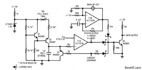
This crystal-controlled integrating A/D converter has a 60-ms conversion time, consumes only 460 μA from a 1.5-V supply, and maintains 10-bit accuracy over a 15°C to 35°C temperature range. To calibrate, apply 0.5000 V to the input and trim the 10-kΩ pot for exactly 1000 pulses out each time the convert-command line is pulsed. No zero trim is required. However, the Q3 inverted 1-mV saturation voltage limits zero resolution to 2 LSBs. (View)
View full Circuit Diagram | Comments | Reading(485)
16_bit_A_D_converter_chopper_stabilized
Published:2009/7/22 21:28:00 Author:Jessie
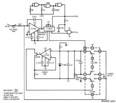
This circuit uses a chopper-stabilized LTC1052 to form a 16-bit A/D converter. To calibrate, apply 5.00000 V and adjust the full-scale trim for 100,000 counts out. Next, set the input to 1.25000 V and adjust the linearity trim for 25,000 counts out. Repeat the procedure until both points are fixed, Converter accuracy is ±1 count with a temperature coefficient of about 15 ppm/°C. (View)
View full Circuit Diagram | Comments | Reading(557)
12_bit_A_D_converter_switched_cotpacitor
Published:2009/7/22 21:15:00 Author:Jessie
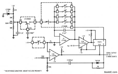
This circuit uses an LTC1043 switched-capacitor to form an economical 12-bit A/D converter. The circuit is self-clocking, has a serial output, and completes a full-scale conversion in 25 ms. Full-scale drift is about 220 ppm/20°C, allowing the circuit to hold 12-bit accuracy over 25°C + 10°C. To calibrate, apply 3 V at the input (non-inverting input of C1B), and trim the gain pot for 4096 pulses output, between data-stream gaps. (View)
View full Circuit Diagram | Comments | Reading(522)
2_kHz_TWO_PHASE
Published:2009/7/6 7:56:00 Author:May
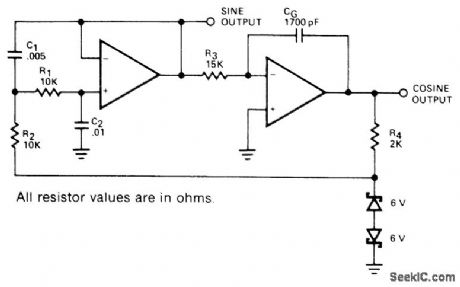
Dual opamp circuit uses two-pole Butterworth bandpass filter followed by phase-shifting single-pole stage that is fed back through zener voltage limiter. Circuit pro-vides simultaneous sine and cosine outputs. Distortion is about 1.5% for sine output and about 3% for cosine. Component values shown are for 741 opamp. For higher frequencies, use 531 opamps to reduce distortion due to slew limiting.- Signetics Analog Data Manual, Signetics, Sunnyvale, CA, 1977, p 642-644. (View)
View full Circuit Diagram | Comments | Reading(1024)
30_kHz_BANDWIDTH
Published:2009/7/6 7:55:00 Author:May
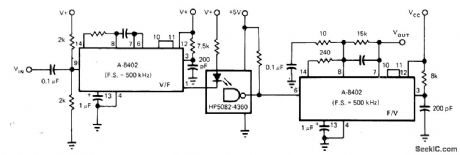
Isolation amplifer circuit uses Intech/Function Modules A-8402 voltage-to-frequency converter having linearity of ±05% to convert input voltage to proportional frequency up to 500 kHz for driving LED of optoisolator. Similar IC converts output of optoisolator back to proportional DC voltage. Supply for conveners is nominally 12 V, but can be 5 to 18 V.-P. Pinter and D. Timm, Voltage-to-Frequency Converters-IC Versions Perform Accurate Data Conversion (and Much More) at Low cost, EDN Magazine, Sept 5, 1977, p 153-157. (View)
View full Circuit Diagram | Comments | Reading(637)
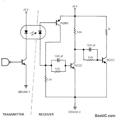
BUILT_IN_HYSTERESIS
Published:2009/7/6 7:54:00 Author:May
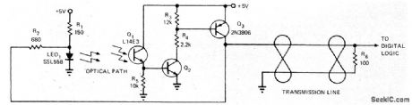
Will operate at all speeds in range from 20 kHz down to zero while still having suitable rise times for driving digital logic. When optical path is blocked, all three transistors are off and output is low. As light on Q1 increases, Q2 and Q3 begin turning on; rising collector of Q3 adds more current through R2 to LED, giving Q1 more light and driving Q1 into saturation. When light dims, Q2 begins to turn off and extra current is cut off, driving Q3 off. With this hysteresis action, there is no constant light level at which circuit will oscillate.-D. C. Hoffman, Optical Sensor Has Built-In Hysteresis, EDN Magazine, June 5, 1973, p 91. (View)
View full Circuit Diagram | Comments | Reading(541)
HUM_BLOCKING_OPTOISOLATOR
Published:2009/7/6 7:52:00 Author:May
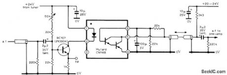
Optoelectronic isolator for audio feed in TV set prevents circulation of ground currents at line frequency, for protection of low-level signal runs from hum interference. Used in tuner providing quality sound and video outputs, circuits for which are given in four-part article. Optoisolator uses light-sensitive Darlington pair in conjunction with infrared-emitting diode. Diode current is adjusted with 50K variable resistor to give best compromise between noise and distortion.-D. C, Read, Television Tuner Design, Wireless World, Jan. 1976, p 51-57. (View)
View full Circuit Diagram | Comments | Reading(717)
Engine Computer Plug-and-Socket Terminal and Instruction Circuits of Beijing Cherokee
Published:2011/7/27 8:19:00 Author:Michel | Keyword: Beijing Cherokee, Plug-and-Socket Terminal, Instruction Circuits

Feet 6 number,wire color, the purpose and connection circuit of engine computer plug-and-socket device are shown as the table.
Table: 2.5 L Petrol Injection Engine Computer Plug-and-Socket Terminal Symbols and Instruction
(View)
View full Circuit Diagram | Comments | Reading(1428)
OPTOISOLATOR_AS_SCANNER
Published:2009/7/6 7:45:00 Author:May
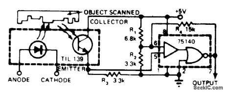
Consists essentially of Texas Instruments TIL 139 source/sensor assembly and common 75140 line receiver. Applications include response to reflected or interrupted light. With 5-V supply, output is at standard TTL levels. To make sensitivity adjustable, insert 500-ohm pot between R1 and R2. To invert output polarity, connect pin 7 of 75140 to pin 3 and take output from pin 1.--W. Grenlund, Low-Cost Photo Scanner Yields High Performance, EDN Magazine, Nov. 20, 1976, p 320. (View)
View full Circuit Diagram | Comments | Reading(836)
BAR_CODE_SIGNAL_CONDITIONER
Published:2009/7/6 7:42:00 Author:May

Processes low-level signal from photodiode of bar-code scanner by converting its current output to volt-age in IC1 for further amplification in IC2. Amplified signal is routed to peak holding circuits that set reference level and to comparator that outputs 0 or 1 based on reference level established. Peak values of white level and black level are held long enough to read through coded bar pattern. Difference between peak values is divided by 2 and fed to one input of comparator, while amplified signal level goes to inverting input. If signal level is greater than reference level, comparator output is 0. If signal level is less than reference level (black bar), output is 1-F. L. Merkowitz, Signal Processing for 0p-tical Bar Code Scanning, BYTE, Dec, 1976, p 77-78 and 80-84. (View)
View full Circuit Diagram | Comments | Reading(2039)
GROUND_ISOLATION
Published:2009/7/6 7:39:00 Author:May
Optoisolator such as HP4320 provides ground isolation up to 200 V between systems used in spacecraft. Arrangement is effective over bandwidth of DC to 1 MHz for both DTL-and TTL-driven circuits.-W. C. Milo, Simple Scheme Isolates System Grounds Optically, EDN Magazine, Sept. 15, 1970, p 64. (View)
View full Circuit Diagram | Comments | Reading(838)
MODULATED_OPTOISOLATOR
Published:2009/7/6 7:38:00 Author:May
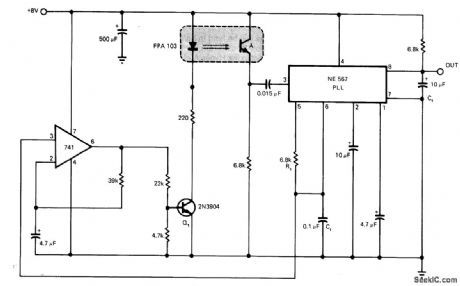
Circuit provides modulation of Fairchild FPA 103 optoisolator at about 1400 Hz and demodulation of signal from detector, to make optoisolator insensitive to strong fluorescent light without compromising performance. Rt and Ct set VCO of NE567 phase4ocked loop IC at about 1400 Hz, and 741 opamp converts triangle wave at pin 6 of PLL to square wave with 50% duty cycle for driving LED of optoisolator through Q1. Also useful with visible light systems.-R. Oliver, Improve Photo Sensors with a Phase-Locked Loop IC, EDN Magazine, April 5, 1976, p 112. (View)
View full Circuit Diagram | Comments | Reading(911)
ANALOG_ISOLATOR_1
Published:2009/7/6 7:36:00 Author:May
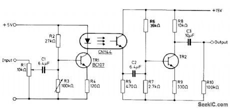
Uses Mullard CNY44 opto-isolator to transmit analog signals between units of equipment having unequal ground potentials. Circuit has 3-dB roll off point at 6 Hz and 80 kHz. Total harmonic distortion at 8 V P-P out-put is less than 1.5% between 100 Hz and 20 kHz. Output transistor TR2 is not critical.- Photocouplers, Mullard, London, 1974, Technical Information 4, TP1477, p 12. (View)
View full Circuit Diagram | Comments | Reading(3851)
DIGITAL_ISOLATION
Published:2009/7/6 7:36:00 Author:May


Optical coupling provides complete electrical isolation between two digital circuits. Input signal as low as +4 V can make output change state, yet circuit safely handles input peaks up to +100 V without breakdown. Q1 and Q2 form current regulator that limits loop current through input of optoisolator to 7 mA. Zener CR2 provides reference voltage that defines current through R2. Schmitt trigger ST1 in output eliminates oscillations that OUTPUT could otherwise occur when slow-rise-time signal is applied to fast TTL circuits. Output changes state when input signal lights LED in optoisolator.-C. E. Mitchell, Optical Coupler and Level Shifter, EDN|EEE Magazine, Feb. 1, 1972, p 55. (View)
View full Circuit Diagram | Comments | Reading(1437)
UPC_WAND_SIGNAL_CONDITIONER
Published:2009/7/6 7:33:00 Author:May
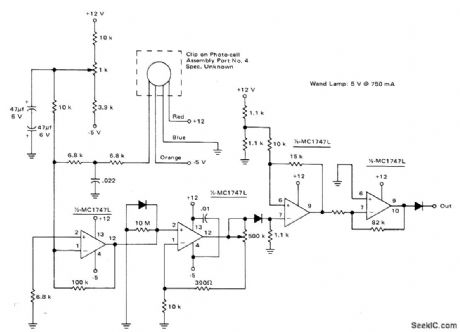
Used in recovering analog output signal of photocell assembly for reading bars of universal productcode. All four sections of two MC1747 dual opamps are used to amplify and condition photocell output so conditioned output of circuit provides TTL level 1 while wand is scanning black and 0 while scanning white. Additional processing is done by microprocessor such as MC6800.- Microprocessor Applications Manual (Motorola Series in Solid-State Electronics), McGraw-Hill, New York, NY, 1975, p 5.16-5-17. (View)
View full Circuit Diagram | Comments | Reading(670)
| Pages:256/471 At 20241242243244245246247248249250251252253254255256257258259260Under 20 |
Circuit Categories
power supply circuit
Amplifier Circuit
Basic Circuit
LED and Light Circuit
Sensor Circuit
Signal Processing
Electrical Equipment Circuit
Control Circuit
Remote Control Circuit
A/D-D/A Converter Circuit
Audio Circuit
Measuring and Test Circuit
Communication Circuit
Computer-Related Circuit
555 Circuit
Automotive Circuit
Repairing Circuit