
Basic Circuit
Index 258
Ratiometric_AID_converter_with_centered_reference_using_resistors
Published:2009/7/22 23:54:00 Author:Jessie

This circuit is similar to that of Fig. 6-13 and 6-15, except that the reference is provided by fixed resistors. Resistors R1 and R2 are selected to provide odd values of reference voltage required by certain transducers (voltages not normally available with adjustable Zeners, such as the LM336). Notice that R3 must be equal to R1, and that both -VREF and +VREF are applied to the ADC through op amps connected for unity gain. (View)
View full Circuit Diagram | Comments | Reading(489)
Ratiometric_A_D_converter_with_mid_supply_centered_reference
Published:2009/7/22 23:46:00 Author:Jessie
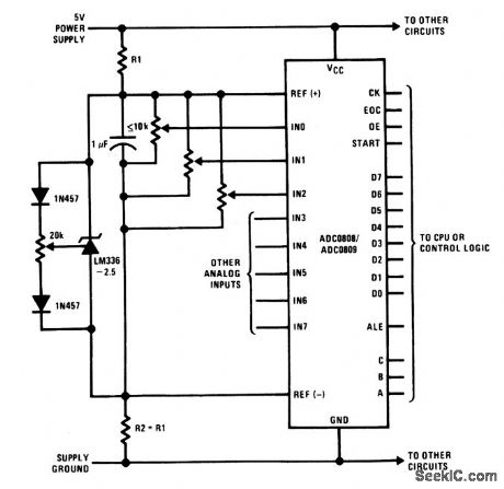
This circuit is similar to that of Fig. 6-13, except that the reference is provided by an LM336 (2.5 V). R1 and R2 should be chosen so that they limit current through the LM336 to about 5 mA, and should track each other over temperature. (View)
View full Circuit Diagram | Comments | Reading(670)
Ratiometric_A_D_converter_zoith_power_supply_reference
Published:2009/7/22 23:08:00 Author:Jessie
This circuit is similar to that of Fig. 6-13, except that the system power Supply is used as a reference. If used, supply noise must be kept to a minimum (with bypassing and separate supply-reference PC traces tapped as close as possible to the supply or regulator). (View)
View full Circuit Diagram | Comments | Reading(484)
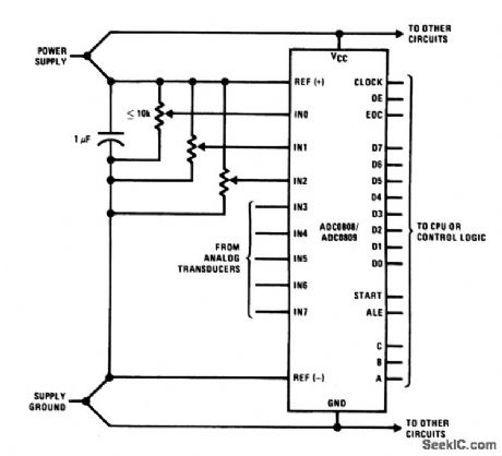
Ratiometric_A_D_converter_with_separate_reference
Published:2009/7/22 23:04:00 Author:Jessie

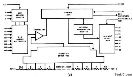
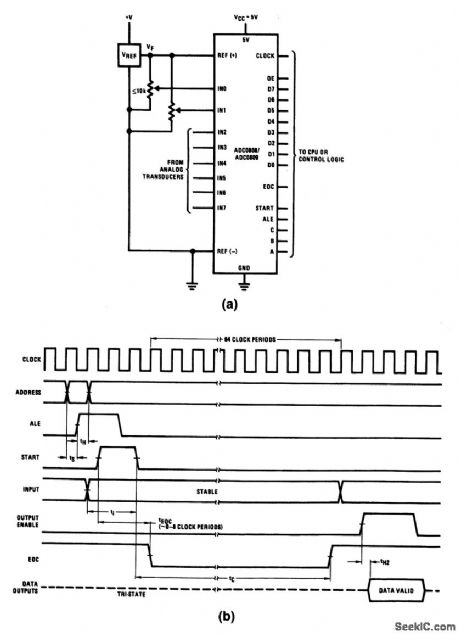

This circuit converts the output from eight ratiometric transducers to an 8-bit digital word using an ADC0808/0809 under control of a CPU or similar digital logic. Figure 6-13B shows the timing between the ADC and the CPU, while Fig. 6-13C shows the internal functions of the ADC. Notice that the ADC includes an SAR, as well as an 8-1 analog multiplexer. (View)
View full Circuit Diagram | Comments | Reading(1151)
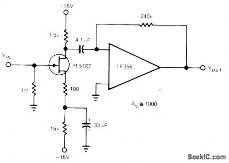
FET_DRIVE
Published:2009/7/6 6:59:00 Author:May

National PF5102 JFET is combined with LF356 opamp to give low noise and high gain, for use as wide-bandwidth AC amplifier. Typical gain for combination shown is about 1000. Any other opamp can be used as long as it meets slew rate and bandwidth requirements.- FET Databook, National Semiconductor, Santa Clara, CA, 1977, p 6-17-6-19. (View)
View full Circuit Diagram | Comments | Reading(1102)
TRAIN_CHUFFER
Published:2009/7/6 6:58:00 Author:May
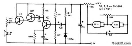
The circuit consists of a white nolse generator which only switches onwith the highpart of the square wave output from the clock circuit. The frequency of the clock ISadjusted with the 10 M pot and the output voltage of the clock IS adjusted by the 100k pot(rate and volume of chuff respectively).The 2M2 pot controls the amount of nolseproduced and the 1 k pot on the speaker controls the pitch of the average nolse. (View)
View full Circuit Diagram | Comments | Reading(690)
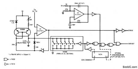
CMOS_A_D_converter_with_serial_output
Published:2009/7/22 22:56:00 Author:Jessie
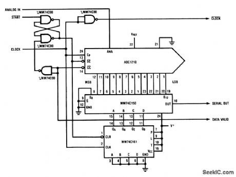
In this circuit, 12 bits of data are shifted out serially using an MM74C150. This permits valid data to be available at the serial output port as fast as half a clock cycle after the most current decision. The data bits are synchronized to the falling edge of the system clock. (View)
View full Circuit Diagram | Comments | Reading(691)
1_A_CURRENT_BOOSTER
Published:2009/7/6 6:58:00 Author:May
Used with LM143 high-voltage opamp to increase output current while providing short-circuit protection and low crossover distortion. With 40-ohm load, output voltage can swing to + 29.6 V and -28 V. All four transistors should be on Thermalloy 6006B or equivalent common heatsink. All diodes are 1N3193.- Linear Applications, Vol. 2, National Semiconductor, Santa Clara, CA, 1976, AN-127, p 4-5. (View)
View full Circuit Diagram | Comments | Reading(919)
ELECTRONICS_BONGOS
Published:2009/7/6 6:57:00 Author:May


This circuit consists of twin-T sine-wave oscillators. Each oscillator has a filter in the feedback loop. If the loop gain is greater than unity, the circuit will oscillate. Gain is adjusted to be just less than unity. Touching the touch plate starts the oscillator, but the moment your finger is removed from the touch plate the oscillations will die away.The rate of decay is a function of circuit gain and controlled by RV1 (and RV3). (View)
View full Circuit Diagram | Comments | Reading(670)
LOW_NOISE_5_kHz
Published:2009/7/6 6:56:00 Author:May
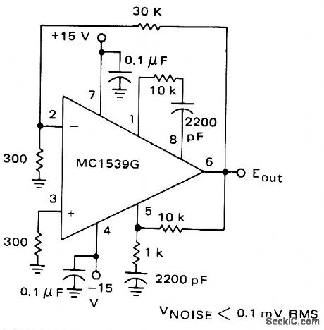
Values shown are for operation of Motorola MC1539G opamp in closed-loop mode with noninverting gain of 100 and source impedance of about 300 ohms. Circuit bandwidth is about 5 kHz.-E. Renschler, The MC1539 Operational Amplifier and Its Applications, Motorola, Phoenix, AZ, 1974, AN-439, p 19. (View)
View full Circuit Diagram | Comments | Reading(551)
60_kHz_PRECISION_RECTIFIER
Published:2009/7/6 6:54:00 Author:May
Usable full-power response of typical opamp is boosted to 60 kHz while giving 300-kHz small-signal band width. Circuit uses transistors to provide speed boosting gain during transition from one precision rectifier diode to the other in feedback loop of opamp. Added stage is driven from power-supply current drains of opamp. Article traces operation of circuit in detail-J. Graeme, Boost Precision Rectifier BW above That of Op Amp Used, EDN Magazine, July 5, 1974, p 67-69. (View)
View full Circuit Diagram | Comments | Reading(697)
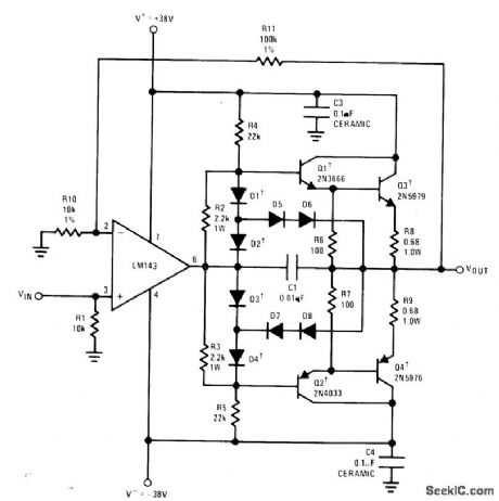
8_A_CURRENT_BOOSTER
Published:2009/7/6 6:53:00 Author:May
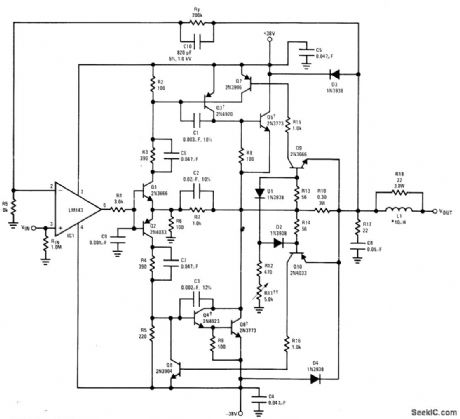
High-compliance power stage for LM143 high-voltage opamp provides very high peak drive currents along with output voltage swings to within 4 V of ±38 V supply under full load. Maximum output current depends on setting of current-adjusting pot R11 and on output voltage. Limit ranges from 14 A when R11 is 0 down to about 4 A for 5K. Maximum power output is 144 WRMS, for which frequency response is 3 dB down at 10 kHz. Voltage gain is 21. Q3-Q6 should be on common Thermalloy 6006B or equivalent heat-sink,- Linear Applications, Vol. 2, National Semiconductor, Santa Clara, CA, 1976, AN-127, p 5-6. (View)
View full Circuit Diagram | Comments | Reading(3027)
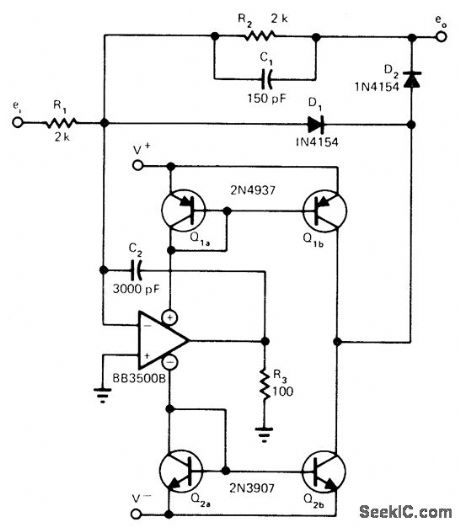
Low_power_10_bit_A_D_converter_1
Published:2009/7/22 22:31:00 Author:Jessie
This circuit is similar to that of Fig. 6-6, except that no external clock is required and typical quiescent power consumption is about 100 μA. Also, the additional ±1 LSB uncertainty of the Fig. 6-6 circuit is eliminated when the flip-flop shown in dashed lines is used. To calibrate, adjust the 50-kΩ pot for 1024 counts with 5.000 V at the input. (View)
View full Circuit Diagram | Comments | Reading(475)
CAPACITANCE_MU_LTIPLIER
Published:2009/7/6 6:49:00 Author:May
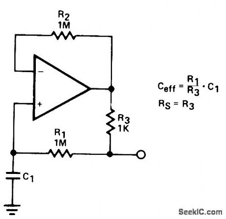
Resistance ratio determines factor by which value of C1 is multiplied when used in simple opamp circuit shown. With values shown, ratio is 1000 and 10-μF capacitor provides effective capacitance of 10,000μF. Q of circuit is limited by effective series resistance, so R1 should be as large as practical. Opamp type is not critical- Signetics Analog Data Manual, Signetics, Sunnyvale, CA, 1977, p 640-641. (View)
View full Circuit Diagram | Comments | Reading(550)
MINIMIZING_PHASE_ERROR
Published:2009/7/6 6:48:00 Author:May
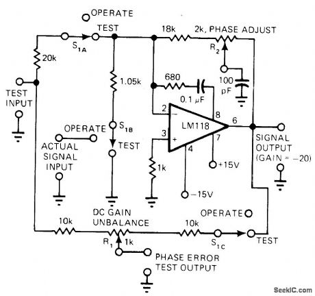
Phase compensation circuit trimmed by R2 keeps phase error of LM118 opamp well below 1° from DC to 200 kHz. In-phase error due to gain peaking is also low. Feed-forward network connected to pin 8 improves stability, making feedback capacitor unnecessary. Step response has about 30% overshoot, and sine response has about +1 dB of peaking before going 3 dB down at about 2 MHz.-R. A. Pease, Technique Trims Op-Amp Amplifiers for Low Phase Shift, EDN Magazine, Aug.20,1977, p 138. (View)
View full Circuit Diagram | Comments | Reading(556)
SINGLE_ENDED_JFET
Published:2009/7/6 6:47:00 Author:May
Basic JFET amplifier is virtually free from popcorn noise problems of bipolar transistors and bipolar-input opamps. Combining JFET transconductance amplifier with current-to-voltage opamp adds high voltage gain and simplifies circuit applications. Gain-limiting 7.5K FET drain resistor is by passed and removed from gain equation. Parameter variation problems are minimized by biasing FET source through 15.1K resistance to negative supply. Gain variations are minimized by leaving 100 ohms of this resistance unby-passed.-L. Maxwell, FET Amplifiers-Take Another Look at These Devices, EDN Magazine, Sept. S, 1977, p 161-163. (View)
View full Circuit Diagram | Comments | Reading(2191)
SIGN_CHANGER
Published:2009/7/6 6:46:00 Author:May
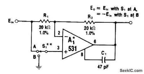
When switch S1 grounds pin 3 of opamp, circuit becomes inverter providing 180° phase shift. When S1 is at position A, input voltage acts on both inputs of A1 and no current flows through R1 and R2; output voltage is then equal to input voltage. Switch permits remote programming of phase reversal. For higher input impedance, 1556 opamp can be used.-W. G. Jung, IC Op-Amp Cookbook, Howard W. Sams, Indianapolis, IN, 1974, p 208-209. (View)
View full Circuit Diagram | Comments | Reading(712)
DEAD_BAND_RESFONSE
Published:2009/7/6 6:45:00 Author:May

With bridge in feed-back loop of opamp, low-level input signals give essentially 100% feedback around A1 so there is very little output voltage. When input current through R1 rises above allowable current limit of circuit, bridge opens and output voltage jumps to new level determined by R2. Input is then amplified by ratio of R2/R1 in normal linear manner. Circuit thus has dead-band property for low levels. Value of R1 sets threshold level.-W. G. Jung, IC Op-Amp Cookbook, Howard W. Sams, Indianapolis, IN, 1974, p 206-207. (View)
View full Circuit Diagram | Comments | Reading(1009)
PRECISE_RECTIFICATION
Published:2009/7/6 6:42:00 Author:May
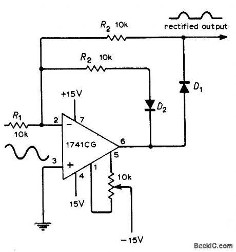
Use of opamp in combination with silicon diode overcomes nonlinearity of diode at forward voltages under about 0.5 V. Offset-voltage pot is adjusted for symmetrical output waveform for small input voltages. D1 is connected in opamp feedback path so initial forward voltage drop required to make diode conduct is supplied by amplifier output. Second feedback path through D2 prevents output saturation on input half-cycles for which Dl is reverse-biased.-G. B. Clayton, Experiments with Operational Amplifiers, Wire-less World, June 1973, p 275-276. (View)
View full Circuit Diagram | Comments | Reading(848)
DIFFERENTIAL_JFET_INPUT
Published:2009/7/6 6:42:00 Author:May
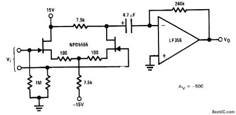
Differential connection of National NPD5565 dual JFET is used when balanced inputs and low distortion are main requirements for AC amplifier, Combination with LF356 opamp shown gives gain of about 500. Noise is somewhat higher than with single-ended JFET.- FET Databook, National Semiconductor, Santa Clara, CA, 1977, p 6-17-6-19. (View)
View full Circuit Diagram | Comments | Reading(1170)
| Pages:258/471 At 20241242243244245246247248249250251252253254255256257258259260Under 20 |
Circuit Categories
power supply circuit
Amplifier Circuit
Basic Circuit
LED and Light Circuit
Sensor Circuit
Signal Processing
Electrical Equipment Circuit
Control Circuit
Remote Control Circuit
A/D-D/A Converter Circuit
Audio Circuit
Measuring and Test Circuit
Communication Circuit
Computer-Related Circuit
555 Circuit
Automotive Circuit
Repairing Circuit