
Basic Circuit
Index 259
POWER_BOOSTER_1
Published:2009/7/6 6:41:00 Author:May

Opamp power booster is used after conventional opamp when greater power-handling capability is required. 741 opamp circuit shown will drive moderate loads. Other opamps may be substituted in power stage if value of R1 is appropriately changed.- Signetics, Analog Data Manual, Signetics, Sunnyvale, CA, 1977, p 640-642. (View)
View full Circuit Diagram | Comments | Reading(2652)
JFET_INPUT
Published:2009/7/6 6:40:00 Author:May
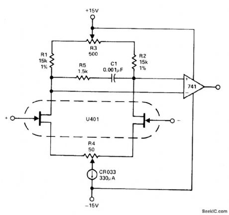
U401 dual JFET acting as preamp for standard bipolar opamp uses CR033 N-channel JFET as 330-pA current source. R4 is used to null initial offset. R3 is adjusted for minimum drift.- Analog Switches and Their Applications, Siliconix, Santa Clara, CA, 1976, p 7-51. (View)
View full Circuit Diagram | Comments | Reading(1961)
1_1000_GAIN_RANGE
Published:2009/7/6 6:39:00 Author:May


Control voltage of 0 to -9 V changes gain of amplifier over complete range while providing maximum output level of 8.5 VRMS and bandwidth of over 20 kHz at maximum gain. If gain range of 100 is sufficient, amplifier can be changed to LM30lA; 20K resistor is then changed to 2K.- Linear Applications, Vol. 2, National Semiconductor, Santa Clara, CA, 1976, AN-129, p 5. (View)
View full Circuit Diagram | Comments | Reading(692)
LOW_TEMPERATURE_COEFFICIENT
Published:2009/7/6 6:36:00 Author:May

Use of National 2N3954 dual FET as input device for opamp gives fast response to thermal transients, making it possible to adjust R3 and R4 so temperature coefficient is less than 5 μV/℃ from -25℃ to +85℃. Common-mode rejection ratio is typically greater than 100 dB for input voltage swings of 5 V, Drain current level is set by Q2 which is 2N5457 FET.- FET Databook, National Semieonductor, Santa Clara, CA, 1977, p 6-4-6-7. (View)
View full Circuit Diagram | Comments | Reading(1290)
POWER_BOOSTER
Published:2009/7/6 6:33:00 Author:May

Simple two-transistor power stage increases power output of LM143 high-voltage opamp. Intended for loads less than 2K. Drawbacks are noticeable crossover distortion and lack of short-circuit protection. Transistors should be used with Thermalloy 2230-5 or equivalent heatsinks.- Linear Applications, Vol. 2, National Semiconductor, Santa Clara, CA, 1976, AN-127, p 3. (View)
View full Circuit Diagram | Comments | Reading(2153)
DIFFERENTIAL_I_O
Published:2009/7/6 6:23:00 Author:May

Arrangement shown for three 741 opamps gives amplifier having differential output as well as differential input. Circuit is designed primarily to drive meter with signal of either polarity when center-tap power supply is not available. Article covers operation and adjustment of circuit.-A. D. Monstall, Differential Input and Output with Op-Amps, Wire-less World, Jan. 1973, p 31. (View)
View full Circuit Diagram | Comments | Reading(725)
BOOSTING_VOLTAGE_RATING
Published:2009/7/6 6:22:00 Author:May

Bootstrapping technique permits operation of low-voltage unity-gain opamp from high-voltage DC supply for handling large input signal voltage swings, while retaining gain and voltage stability of opamp. Allowable input-voltage range depends entirely on transistor rating. With 1000-V transistors, circuit can handle input signals of ±475 V. Input capability for values shown is ±100 V P-P for DC to 10 kHz. Output capability is 5 mA P at t 100 V. Input impedance is 10 teraohms. -S. A. Jensen, High-Voltage Source Follower, EDN IEEE Magazine, Feb. 1, 1972, p 58. (View)
View full Circuit Diagram | Comments | Reading(1620)
CMOS_A_D_converter_with_positive_true_logicbipolar__VSUBREF_SUB_to___VSUBREF_SUB
Published:2009/7/22 22:50:00 Author:Jessie

This circuit is similar to that of Fig. 6-8, except that the output is positive-true -VREF to + VREF. (View)
View full Circuit Diagram | Comments | Reading(538)
100_mA_CURRENT_BOOSTER
Published:2009/7/6 6:20:00 Author:May

Provides short-circuit protection along with current boosting for LM143 high-voltage opamp. Diodes are 1N914. Use Thermalloy 2230-5 or equivalent heatsinks, with transistors Output is± 33 V P-P into 400-ohm load.-“Linear Applications, Vol. 2,” National Semiconductor, Santa Clara, CA, 1976, AN-127, p 4. (View)
View full Circuit Diagram | Comments | Reading(2065)
CMOS_A_D_converter_with_positive_true_logic_0_V_to___VSUBREF_SUB_input
Published:2009/7/22 22:47:00 Author:Jessie

This circuit is similar to that of Fig. 6-8, except that the output is positive-true 0 V to + VREF. (View)
View full Circuit Diagram | Comments | Reading(527)
CMOS_A_D_converter_with_complementary_logic_bipolar__VSUBREF_SUB_to___VSUBREF_SUB
Published:2009/7/22 22:42:00 Author:Jessie
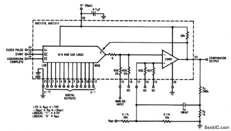
This circuit is similar to that of Fig.6-8, except that the output is bipolar -VREF to + VREF. (View)
View full Circuit Diagram | Comments | Reading(514)
PUNCHED_TAPE_READER
Published:2009/7/6 6:06:00 Author:May
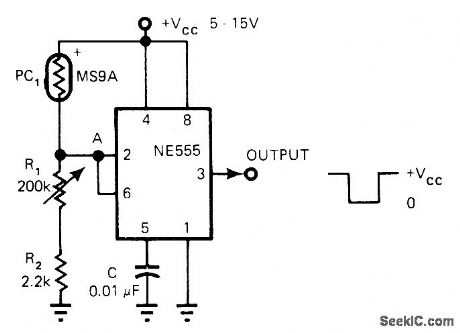
Connection of 555 timer as Schmitt trigger produces output pulses with sharp rise and fall times that are independent of tape speed. Output is compatible with TTL or CMOS circuits. When scanning light beam hits hole in punched card or tape, resistance of light-sensitive resistor drops sharply and voltage at pins 2 and 6 rises above 0.67 VCC. Voltage at output pin 3 then drops sharply from VCC to 0 V. When PC1 goes dark, circuit switches rapidly back to original state. Reverse PC1 and R1-R2 for positive edge-triggered logic.-S. Sarpangal, 555 Timer Implements Tape Reader, EDN Magazine, Jan. 5, 1978, p 86 and 90. (View)
View full Circuit Diagram | Comments | Reading(1747)
RATIO_OF_TWO_UNKNOWNS
Published:2009/7/6 6:03:00 Author:May
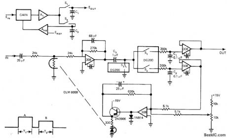
Developed for use when two signals are time-shared on same input line, such as exists when two LEDs alternately illuminate single photocell. Measures ratio of amplitudes of unknowns with accuracy better than 1%. During time period T1, input is sampled through s2 and stored on C2 for comparison with reference voltage Result is applied through switch able amplifier network AFB to gain control element which is LED-photoresistor coupled pair (CLM 6000) This closed loop adjusts signal gain to make denominator of ratio equal to reference voltage. Numerator, corresponding to time T2, is multiplied by-same gain so numerator output is proportional to de-sired ratio B/A of unknowns. Article describes circuit operation in detail.-R. E. Bober, Here's a Low-Cost Way to Measure Ratios, EDN Magazine, March 5, 1976, p 108, 110, and 112. (View)
View full Circuit Diagram | Comments | Reading(528)
LOW_BATTERY_WARNING_DISCONNECTOR
Published:2009/7/6 5:59:00 Author:May

NiCad batteries are excellent rechargeable power sources for portable equipment, but care must be taken to ensure that the batteries are not damaged by overdischarge. Specifically, a NiCad battery should not be discharged to the point where the polarity of the cell is reversed and is reverse-charged by the higher-capacity cells. This reverse charging will dramatically reduce the life of a NiCad battery. This circuit both prevents reverse charging and also gives a low-battery warning. A typical low-battery warning voltage is 1 V per cell. Since a NiCad, 9-V battery is ordinarily made up of six cells with a nominal voltage of 7.2 V, a low-battery waming of 6 V is appropriate, with a small hysteresis of 100 mV. To prevent overdischarge of a battery, the load should be disconnected when the battery voltage is 1 V x (,N- 1), where N = number of cells. In this case, the low-battery load disconnect should occur at 5 V. Since the battery voltage will rise when the load is disconnected, 800 mV of hysteresis is used to prevent repeated on-off cycling. (View)
View full Circuit Diagram | Comments | Reading(665)
BASIC_COLOR_ORGAN
Published:2009/7/6 5:58:00 Author:May

Transformer T1 can be any matching transistor type in the range of 500/500 to 2500/2500 ohms. No connections from the SCR or its components are connected to ground. For safety's sake, keep the 117-V line voltage from the amplifier connections-that is the reason for using T1. To adjust, set potentiometer R1 off and adjust the amplifier volume control for a normal listening level. Then adjust the potentiometer until the lamp starts to throb in step with the beat. (View)
View full Circuit Diagram | Comments | Reading(613)
COLOR_ORGAN
Published:2009/7/6 5:56:00 Author:May
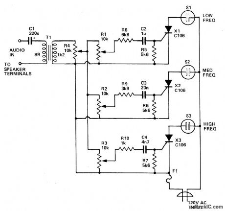
Three lights are controlled by the three channels. One light will pulse in response to the bass, another illuminates with midrange sounds, and the last lights for high notes.Four level controls allow adjustment of overall light level and each channel individually.Up to 200 watts per channel can be handled. (View)
View full Circuit Diagram | Comments | Reading(1969)
__VOX_BOX
Published:2009/7/6 5:55:00 Author:May
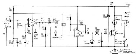
The electronic circuit in the VOX Box consists of three parts: a microphone preamplifier, a Schmitt trigger, and a relay driver. Input signals (MIC INPUT terminals) to the microphone preamplifier (U1) are amplified and fed to a THRESHOLD control (R8). When the preselected threshold voltage level is exceeded, the output of the Schmitt trigger (U2) immediately goes high. The signal from U2 is rectified and the voltage developed across C7 turns on the relay energizer transistor (Q1). That transistor action passes pull-down current through the coil of relay K1. The changing of the relay SPDT contacts can be used to either make or break an external ac or dc circuit.
(View)
View full Circuit Diagram | Comments | Reading(2057)
SOUND_ACTIVATED_ac_SWITCH
Published:2009/7/6 5:54:00 Author:May
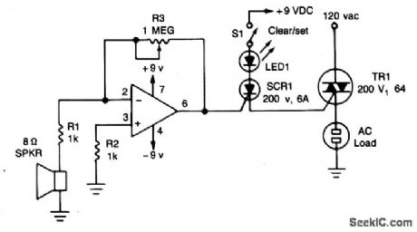
The circuit uses a 741 op amp operating as an inverting amplifier to amplify the voltage produced by an 8-ohm speaker used to detect any sounds. The feedback resistor R3, a 1-megohm potentiometer used to vary the gain of the amplifier determines the sensitivity of the circuit. When S1 is closed in the (SET) position and a sound is applied to the speaker, SCR1 is tumed on. It will remain in conduction until the anode voltage is removed by opening S1, putting it in its RESET position. (Once an SCR is turned on, the gate or trigger has no control over the circuit.) As long as the SCR conducts,the Triac, TR1, will remain on and supply voltage to the logd. (View)
View full Circuit Diagram | Comments | Reading(818)
PREAMP_WITH_EQUALIZATION
Published:2009/7/6 5:52:00 Author:May
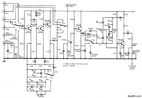
Baaed on 1966 high-performance Bailey preamp design with improved filter and tone control circuits and additional complete ceramic-pickup equalizing circuit. Equalization for magnetic pickups and other types of inputs is automatically selected by three-deck input selector switch. To avoid overloading input stage, adjust set level control to give comfortable listening level for given input when main volume control is at about half its maximum rotation. Article also gives lower-cost version for ceramic-pickup equalization and changes required in this for operation from negative supply.-B. J. Bur-rows, Ceramic Pickup Equalization, Wireless World, Aug. 1971, p 379-382. (View)
View full Circuit Diagram | Comments | Reading(1833)
RUMBLE_FILTER_1
Published:2009/7/6 5:51:00 Author:May

Used to roll off low-frequency noise associated with worn turntable and tape transport mechanisms. Gain is 1. Design procedure is given. For values shown, corner frequency is 50 Hz and slope is -12 dB per octave.- Audio Handbook, National Semi-conductor, Santa Clara, CA, 1977, p 2-49-2-52. (View)
View full Circuit Diagram | Comments | Reading(814)
| Pages:259/471 At 20241242243244245246247248249250251252253254255256257258259260Under 20 |
Circuit Categories
power supply circuit
Amplifier Circuit
Basic Circuit
LED and Light Circuit
Sensor Circuit
Signal Processing
Electrical Equipment Circuit
Control Circuit
Remote Control Circuit
A/D-D/A Converter Circuit
Audio Circuit
Measuring and Test Circuit
Communication Circuit
Computer-Related Circuit
555 Circuit
Automotive Circuit
Repairing Circuit