
Basic Circuit
Index 257
ISOLATION_WITH_GAIN_COMPENSATION
Published:2009/7/6 7:32:00 Author:May

Provides total harmonic distortion under 1% while automatically adjusting for temperature-produced or other DC gain variations in opto-isolator. Output signal is sampled and fed back to FET to maintain constant AC gain. Design equations are given.-A. Billings, Optocoupler Provides Analog Isolation, EDN Magazine, Nov. 5, 1978, p 121-122. (View)
View full Circuit Diagram | Comments | Reading(561)
ANALOG_ISOLATOR
Published:2009/7/6 7:30:00 Author:May

Circuit is basically FM transmission system in which light is used as transmission medium. Transmitter uses 565 PLL as VCO for flashing LED of optoisolator at rate proportional to input voltage. Phototransistor drives amplifier having sufficient gain to apply 200 mV p-p singnal to input of receiving 565 acting as FM detector for re-creating input to transmitter. Supply can be ±6 V to ±12 V.- Signetics Analog Data Manul, Signetics, Sunnyvale, CA, 1977, p 846-847. (View)
View full Circuit Diagram | Comments | Reading(1349)
ASTABLE_MULTIVIBRATOR
Published:2009/7/6 7:24:00 Author:May

The circuit with independent control of ON and OFF periods uses the CA3130 BiMOS op amp for filters, oscillators, and long-duration timers. With input current at 50 pA, oscillators can utilize large-resist or/small-capacitor combinations without loading effects.
(View)
View full Circuit Diagram | Comments | Reading(3245)
SET_TESET_LATCH
Published:2009/7/6 7:23:00 Author:May
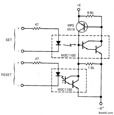
Provides almost complete isolation between each input and the output, as well as between inputs. Applying 2-V pulse at 14 mA momentarily to SET terminals allows up to 150 mA to flow between output terminals. This current flows until about 2 V at 15 mA is appkied to REST terminals or untilload voltage is reduced enough to drop load current below 1 mA.-R.N. Dotson, Set-Reset Latch Uses Optical Couplers, EDN Magazine, Jan.5, 1973, p 107. (View)
View full Circuit Diagram | Comments | Reading(626)
DC_ISOLATOR_WITH_HARMONIC_SUPPESSION
Published:2009/7/6 7:19:00 Author:May
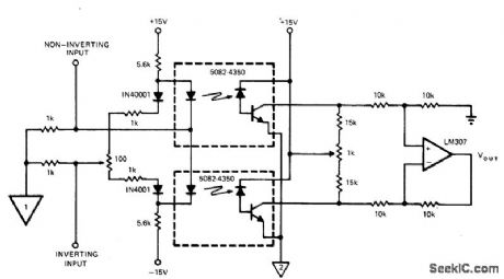
Two isolators operating like push-pull amplifier minimize harmonic generation. When input signal is applied, upward change of incremental gain in one isolator is balanced by downward change in other to give harmonic cancellation. Circuit gain is about unity. Bandwidth is 2 MHz for signal below 2 V p-p. Input signals of either polarity may be applied at either inverting or noninverting input.-H. Sorensen, Opto-Isolator Developments Are Making Your Design Chores Simpler, EDN Magazine, Dec. 20, 1973, p 36-44. (View)
View full Circuit Diagram | Comments | Reading(641)
OPTICAL_DRIVE_FOR_SWITCHING_TRANSISTOR
Published:2009/7/6 7:17:00 Author:May
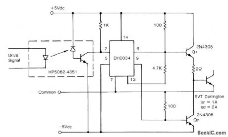
Base driver circuit for TRW SVT6062 power Darlington switching transistor uses separate isolated bias supplies for each transistor to provide performance characteristics of driver transformer at lower cost. Bias supplies can use small 60-Hz transformers with bridge rectifiers and light filtering. Control isolation is provided by high-speed optical coupler that can be controlled directly from logic. DH0034 IC amplifies coupler output and provides level shifting as required for driving transistors Q1 and Q2.-D. Roark, Base Drive Considerations in High Power Switching Transistors, TRW Power Semiconductors, Lawndale, CA, 1975, Application Note No. 120, p 8. (View)
View full Circuit Diagram | Comments | Reading(944)
OSCILLATOR_WITH_FREQUENCY_DOUBLED_OUTPUT
Published:2009/7/6 7:14:00 Author:May
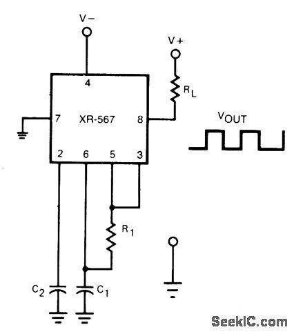
The current-controlled oscillator frequency can be doubled by applying a portion of the square-wave output at pin 5 back to the input at pin 3, as shown. In this manner, the quadrature detector functions as a frequency doubler and produces an output of 2 f0 at pin 8. (View)
View full Circuit Diagram | Comments | Reading(472)
Digital Multimeter Electric Block Circuit with Constant Current Source
Published:2011/7/27 10:10:00 Author:Michel | Keyword: Digital Multimeter, Block Circuit, Constant Current Source
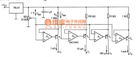
The digital multimeter electric block diagram with constant current source is shown as above.The electrical resistance measuring principle in the digital multimeter is that measured resistance is used to generate voltage with constant current.Constant current source adopts 4 op-amp MC3403,UREF=1V is set by RP1 (2 Ok Ω resistance).The constant current output is IREF=UREF/Rs,thus,when Rs=1MΩ,IZ is 1μA,when Rs=1OOkΩ,IY is 10μA,when Rs=1OkΩ,IX is 100μA and Iw is 1 mA when Rs=1kΩ. (View)
View full Circuit Diagram | Comments | Reading(1770)
BAR_CODE_READER
Published:2009/7/6 7:13:00 Author:May

Edge-sensitive circuit outputs short pulses at each black-to-white or white-to-black transition. Timing diagram shows outputs corresponding to bar-code pat-tern indicated. Direct-current level at base of Q1 is held constant by DC servo action despite changes in temperature, ambient light, or back-ground of pattern. Alternate sensor uses photodiode and 2N2222 transistor for increased bandwidth. Amplified differentiated signal from collector of a2 is further amplified by IC2 and fed to dual threshold comparator. Output of comparator is short pulse for each transition, suitable for feed to microprocessor.-F. L. Merkowitz, Signal Processing for Optical Bar Code Scanning, BYTE, Dec. 1976, p 77-78 and 80-84. (View)
View full Circuit Diagram | Comments | Reading(4297)
FULL_WAVE_RECTIFIER
Published:2009/7/6 7:11:00 Author:May
Circuit provides accurate full-wave rectification of input signal, with distortion below 5% up to 10 kHz. Reversal of all diode polarities reverses polarity of out-put. Output impedance is low for both input polarities, and errors are small at all signal levels.- Signetics Analog Data Manual, Signetics, Sunnyvale, CA, 1977, p 641-643. (View)
View full Circuit Diagram | Comments | Reading(912)
P012404UD Frequency Synthesizer Integrated Circuit
Published:2011/7/27 9:55:00 Author:Michel | Keyword: Frequency Synthesizer, Integrated Circuit
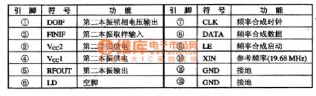
P012404UD is a kind of frequency synthesizer integrated circuit which is widely used in samsung mobile phones, such as CDMA series samsung A599 cell phones, etc.
First,Functions FeaturesPO12404UD integrated circuit contains the second phase lock voltage circuit,second vibration vibration power supply circuit, data circuit, frequency synthesis start-up circuit, reference frequency circuit and some auxiliary function circuit.
Second,Pins FunctionsPO12404UD integrated circuits uses 12 feet 4 columns encapsulation.And pins functions of frequency synthesis clock circuit and its integrated circuit are shown as table 1.
Table 1:PO12404UD IC Pins Functions (View)
View full Circuit Diagram | Comments | Reading(423)
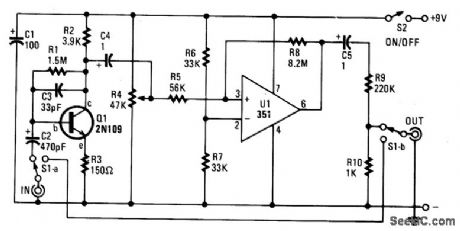
_FUNK_BOX
Published:2009/7/6 7:10:00 Author:May
Adjusting potentiometer R7 adds extra twang from way down low to way up high.To set the unit,adjust potentiometer R4 until you hear a whistle (oscillation); then back off R4 until the oscillation just ceases. The effect can be varied from bass to treble by R7.
(View)
View full Circuit Diagram | Comments | Reading(492)
TWANG_TWANG_CIRCUIT
Published:2009/7/6 7:07:00 Author:May
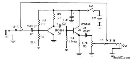
Twang is a guitar sound that more or less approximates a banjo or mandolin. The circuit produces unusual sounds from an ordinary electric guitar by cutting the bass, severely distorting the midband and highs, and then amplifying the distortion. S1 cuts the effect in and out, S2 turns the unit on and off.
(View)
View full Circuit Diagram | Comments | Reading(781)
1000_GAIN_AT_2_kHz
Published:2009/7/6 7:06:00 Author:May
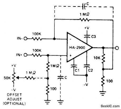
Uses Harris HA-2900 chopper-stabilized opamp. Either input terminal may be grounded, giving choice of inverting or noninverting operation, or inputs may be driven differentially. Symmetrical input networks eliminate chopper noise, limiting total input noise to about 30μ VRMS when C is 0. Noise can be further reduced, at expense of bandwidth, by adding optional capacitors C as shown. Without these capacitors, bandwidth is 2 kHz.- Linear & Data Acquisition Products, Harris Semiconductor, Melbourne, FL, Vol. 1, 1977, p 7-69 (Application Note 518). (View)
View full Circuit Diagram | Comments | Reading(591)
PRECISION_ABSOLUTE_VALUE
Published:2009/7/6 7:05:00 Author:May
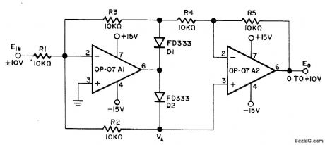
Circuit using two Precision Monolithics OP-07 opamps provides precise full-wave rectification by inverting negative-polarity input voltages and operating as unity-gain buff er for positive-polarity inputs. Applications include positive-peak detectors, single-quadrant multipliers, and magnitude-only measuring systems. For positive inputs, circuit simply operates as two unity-gain amplifier stages. Negative input turns D1 off and D2 on, changing resistor currents precisely enough to give overall circuit gain of -1. Design equations are given.-D. Soderquist and G. Erdi, The OP-07 Ultra-Low Offset Voltage Op Amp-a Bipolar Op Amp That Challenges Choppers, Eliminates Nulling, Precision Monolithics, Santa Clara, CA, 1975, AN-13, p 10. (View)
View full Circuit Diagram | Comments | Reading(3536)
UNUSUAL_FUZZ
Published:2009/7/6 7:05:00 Author:May
It seems that guitar fuzz boxes have been around since the beginning of rock, and have seen little improvement over the years. This one is somewhat different because rather than simply distorting the sound, it also pulses in step with the peaks of the waveform from the pickup because of the Schmitt trigger op amp circuit. Capacitor C2 requires some explanation. It should normally be a 1- or 2-μF electrolytic capacitor. However, we show the value as 470 pF because it's recommended as an experimental value giving fgr out effects.
(View)
View full Circuit Diagram | Comments | Reading(856)
WAA_WAA_CIRCUIT
Published:2009/7/6 7:04:00 Author:May

The waa-waa effect is achieved as certain frequencies are amplified more than others.A phase shift RC oscillator makes up the basic circuit. Negative feedback is obtained by feeding part of the signal back to the base. When adjusting initially, RV1 is turned to minimum. RV2 is adjusted to a point at which an audible whistle appears indicating oscillation. RV1 is then adjusted till the oscillation just disappears. It should be possible to set RV2 to any value without any oscillation, this should also be achieved with the minimum possible value of RV1. (View)
View full Circuit Diagram | Comments | Reading(939)
STEAM_LOCOMOTIVE_WHISTLE
Published:2009/7/6 7:02:00 Author:May

The waveform of a steam whistle is a complex combination of white noise and an audio frequency oscillation. The noise generator is a transistor (Q1) biased into zener mode. The audio frequency oscillation is a straightforward mixture of two similar (but not identical) sine waves, which after their addition produce a more complex waveshape.The sine wave generators are twin-t oscillators. Preset RV1 mixes the two sine waves so that an appropriate waveform is obtained. RV2 mixes this waveform with the white noise. Adjustment of all three presets will result in the required sound. Integrated circuit IC1 is an operational amplifier used as a simple mixer/amplifter which combines the steam whistle, chuffer, (generated elsewhere) and two-tone horn sounds into one, suitable for amplification by an extemal amplifier.
(View)
View full Circuit Diagram | Comments | Reading(2879)
A_D_converter_for_nonratiornetric_transducer_inputs_buffered
Published:2009/7/23 0:43:00 Author:Jessie
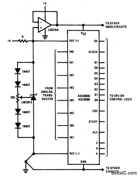
This circuit is similar to that of Fig. 6-17, except that the supply is buffered through an op-amp connected for unity gain. This isolates the ADC reference from the ADC supply (as well as from other system components).
(View)
View full Circuit Diagram | Comments | Reading(468)
BIRD_CHIRP
Published:2009/7/6 7:00:00 Author:May
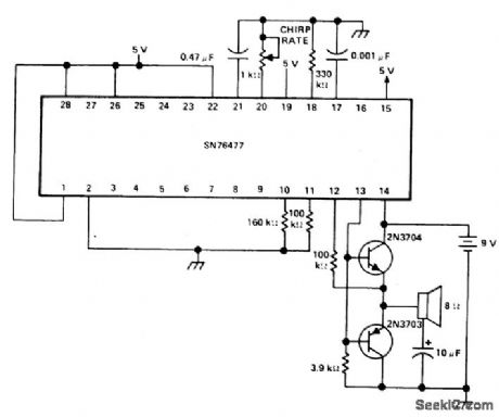
For a barking dog,the capacitor at pin 17 o changed to 15 pF to mcrease the frequency of the VCO.
(View)
View full Circuit Diagram | Comments | Reading(855)
| Pages:257/471 At 20241242243244245246247248249250251252253254255256257258259260Under 20 |
Circuit Categories
power supply circuit
Amplifier Circuit
Basic Circuit
LED and Light Circuit
Sensor Circuit
Signal Processing
Electrical Equipment Circuit
Control Circuit
Remote Control Circuit
A/D-D/A Converter Circuit
Audio Circuit
Measuring and Test Circuit
Communication Circuit
Computer-Related Circuit
555 Circuit
Automotive Circuit
Repairing Circuit