
Basic Circuit
Index 245
ASTABLE
Published:2009/7/7 6:21:00 Author:May
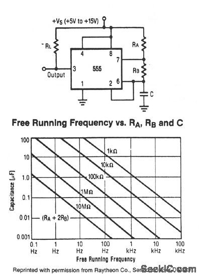

This astable will trigger itself and run free as a multivibrator. The external capacitor charges through RA and RB and discharges through RB only. Thus, the duty cycle is set by the ratio of these two resistors, and the capacitor charges and discharges between 1/3 VS and 2/3 VS. The charge and discharge times, and therefore frequency, are independent of supply voltage. The free-running frequency versus RA, RB and C is shown in the graph. (View)
View full Circuit Diagram | Comments | Reading(1100)
LOW_POWER_WIDE_RANGE_PROGRAMMABLE
Published:2009/7/7 6:19:00 Author:May
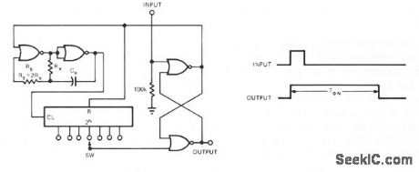
This CMOS circuit can be used as a 1-shot time delay switch and general-purpose timer. The circuit consists of a gated oscillator and a latch made from one CD4001 quad 2-input NOR gate as shown and a CD4020 14-stage counter. TON is a function of the oscillator frequency from the RxCx and the proper 2N output from the counter. A pulse applied to the latch will enable the oscillator and counter. The latch output will remain high until the 2N count resets the latch and disables the oscillator and counter. The circuit provides μs to hour interval timing. The extraordinarily long periods available from the CMOS oscillator, combined with the 14-stage counter, make this range possible. Further decoding is required for variations finer than a power of two. (View)
View full Circuit Diagram | Comments | Reading(632)
UP_DOWN_COUNTER_EXTREME_COUNT_FREEZER
Published:2009/7/7 6:12:00 Author:May
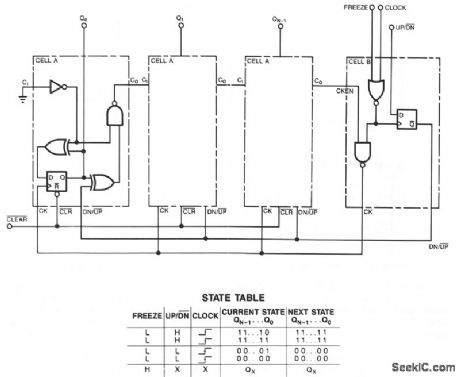
The discrete-gate up/down-counter design has the unusual property of freezing, or saturating, when it reaches its lowest count in the down-count mode or its highest count in the count-up mode instead of rolling over and resetting as do most counters. This property proves especially useful in position-control systems. For example, you wouldn't want a robot's arm to slowly move to full extension as the counter counts up and then have it suddenly slam back to its rest position when the counter resets to zero.
You can cascade as many of the A cells as you need because the counter's outputs are synchronous.The B cell accepts the carry bit from the most significant bit's A cell and provides the clock control that stops the counter. Make sure that the freeze input to the B cell doesn't get asserted when the clock input is low; otherwise, the counter might make an extra count.
(View)
View full Circuit Diagram | Comments | Reading(598)
TOUCHOMATIC
Published:2009/7/7 5:39:00 Author:May
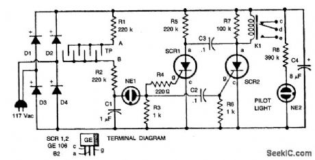
When someone touches the touchplate (TP), the resistance of his finger across points A and B is added in series to the combination of R1 and R2, the capacitor C2 begins to charge. When the voltage across C1 is finally sufficient to fire NE1, C1 will begin to discharge. When NE1 fires, it produces a short between its terminals. Since R3 is connected across C1, they are effectively in series after NE1 fires. A voltage spike will then be passed by C2 and this will act as a positive triggering pulse. The pulse is fed to both SCR gates: SCR2 conducts, there by closing relay K1. With a finger no longer on the touchplate, no more pulses are forthcoming because the C1 charge path is open.The next contact with the touchplate will produce a pulse which triggers SCR1. SCR2 is now off by capacitor C3 which was charged by current passing through R6 and SCR2.The firing of SCR1 in this way places a negative voltage across SCR2 which momentarily drops the relay current to a point below the holding current value of SCR2. (Holding current is the minimum current an SCR requires to remain in a conducting state once its gate voltage is removed.) With SCR2 turned off, the relay will open and SCR1 will turn off due to the large resistance in series with its anode. Starved in this way SCR1 turns off because of a forced lack of holding current. (View)
View full Circuit Diagram | Comments | Reading(753)
2_3O_MHz_3OO_W_LlNEAR
Published:2009/7/7 5:34:00 Author:May
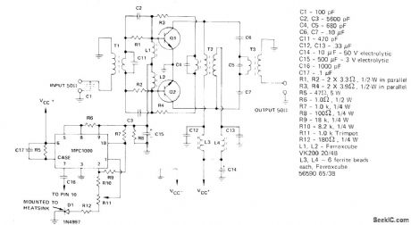
Motorola MRF422 high-power transistors connected in push-pull provide 300 W of PEP or CW output power across band. Uses MPC1000 regulator rated for 10 A and dissipation of 100 W with proper heatsink. Since average base current of transistors is less than 500 mA, however, regulator can be used without heatsink. T1 and T3 have 9:1 impedance ratio, obtained with 1/8-inch copper-braid secondary through which 3 turns of No.22 are wound for primary on Stackpole dual balun ferrite core 57-1845-24B. T2 has 5 turns of two twisted pairs No. 22 enamel wound on Stackpole 57-9322 toroid.-H. Granberg, Get 300 Watts PEP Linear Across 2 to 30 MHz from This Push-Pull Amplifier, Motorola, Phoenix, AZ. 1978, EB-27. (View)
View full Circuit Diagram | Comments | Reading(3366)
AMPLIFIED_ZENER
Published:2009/7/7 5:31:00 Author:May
Combination of 1-W zener and 50-90 W audio trnsistor replaces 50-W zener in developing bias ror high-power tubetype linear amplifier Voltage of zener should be about 0.3 V less than desired bias voltage if using germanium transistor and about 0.7 V less for silicon transistor. Connec-tions are shown for PNP and PNP transistors.Use chassis as heatsink for transistor, with mica insulating washer for NPN. Ferrite beads dis-courage parasitic oscillations.-An Altemative to High-Wattage Zener Diodes, QST, June 1975, p45. (View)
View full Circuit Diagram | Comments | Reading(778)
432_450_MHz
Published:2009/7/7 5:27:00 Author:May
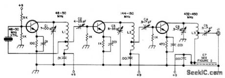
Crystal oscillator stage operating at 48-50 MHz puts out enough power to drive pair of triplers. All transistors are HEP-75.L1 is 20 turns No. 24 on 5-mm form, tapped 8 turns from cold end. L2 is 5 turns No. 20 airwound to 8-mm diameter. L3 is 3 turns No, 20 air-wound to 5-mm diameter, with center tap. rticle covers construction, adjustment, and uses,-B. Hoisington, Getting Started on 450 MHz, 73 Magazine, Nov. 1973, p 21-24. (View)
View full Circuit Diagram | Comments | Reading(645)
ANALOG_SUMMING
Published:2009/7/7 5:24:00 Author:May

ON/OFF programming ofμA776 opamps allows any or all inputs to be on at given time. Switched outputs are combined in summing inverter A,. Voltage followers A1-A3 are programmed from on to off by Q1-Q3 and A5- A7. Noise gain of stage A4, is minimized when input channel is switched off. If sign inversion by A4, is undesirable, add inverter stage following A.. Any number of additional channels can be added. Programming pulses are applied to inputs of A,, A6, and A,.-W. G. Jung, IC 0p-Amp Cookbook, Howard W Sams, Indianapolis, IN, 1974, p 419-421. (View)
View full Circuit Diagram | Comments | Reading(648)
TWO_INPUT_FSK_MULTIPLEXER
Published:2009/7/7 5:15:00 Author:May

Uses Signetics NE571 or NE570 analog compandors. Gain of each channel is unity, as determined by RGAIN value for channel. When complementary control signals are provided, FSK generator switches between the two signal inputs. Outputs, when on, are summed by opamp in IC. Each channel is gated off by low control logic input. For FSK or alternate-channel ';'' C0N-TR0L A and CONTROL B signals should be com plementary. Control signal suppression is optimized with chopper null pot. Suppression is better than 60 dB after trimming. Circuit can also be used as summing switch, with both signals on at any given instant.-W. G. Jung, Gain Control IC for Audio Signal Processing, Ham Radio, July 1977, p 47-53. (View)
View full Circuit Diagram | Comments | Reading(1216)
10_V_TEMPERATURE_STABILIZED
Published:2009/7/7 5:10:00 Author:May

Self-regu lation of substrate temperature of CA3046 fivetransistor chip allows 10-V reference output voltage to rlse only 0.5 mV when temperature increases from 27 to 62℃ Circuit requires only single 15-V supply Zener-connected transistor Q2 and diode-connected transistor Q1 together provide temperature compensation by sensing voltage across Q1 (DS) and comparing it with temperature-reference voltage produced across R1 by μA741G opamp A1. Opamp drives Q5 to control current through Q4 which serves as chip heater. Opamp A2 (μA741G) and asso-ciated components (including Q1-Q2 in feedback path) act as self-regulating (zener-current) voltage reference.-M. J. Shah, A Self-Regutating Temperature-Sta bil ized Reference, EDN Maga-zine, May 20, 1974, p 74 and 76. (View)
View full Circuit Diagram | Comments | Reading(1658)
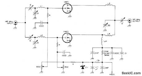
TRANSISTORS_FOR_DRIVER_TUBES
Published:2009/7/7 5:08:00 Author:May

Solidstate replacement for 12BY7A power amplifier runs much cooler than tube. Shield is required between input and output circuits. Gate 2 is biased very high and gate 1 is close to source voltage, to permit maximum signal range with-out changing parameters. Bypassed zener VR9 prevents 100-V collector signal swing from exceeding transistor breakdown voltage. Solidstate replacements for other tube types in Drake T-4XB transmitter are also given in arti-cle.-H. J. Sartori, Solid-Tubes-a New Life for Old Designs, 057, April 1977, p 45-50. (View)
View full Circuit Diagram | Comments | Reading(1495)
0_360°to_0_180°
Published:2009/7/7 5:05:00 Author:May

Used for converting angular information in 36O° wrap-around code to ±180°sign-plus-magnitude code. For values under 180°, converter outputs and inputs are identical. For larger input angles, output code is complement of input plus one. Used for interfacing shaft encoders and synchro-to-digital converters to digital display. Article gives truth table showing which lines are high and which are low at input and at output for angular increments of 22.5°.-J. N. Phillips, Convert Wrap-Around Code to Sign-Plus-Magnitude, EDN Magazine, Jan. 5, 1973, p 103. (View)
View full Circuit Diagram | Comments | Reading(518)
TEN_BAND_GRAPHIC_EQUALIZER,USING_ACTIVE_FILTERS
Published:2009/7/7 5:04:00 Author:May


The above circuit is repeated ten times. Use the table to calculate values. (View)
View full Circuit Diagram | Comments | Reading(609)
V_F_GIVES_10_to_10000_Hz
Published:2009/7/7 5:02:00 Author:May

Current proportional to input voltage is balanced via periodic charging of C1 to precisely repeatable voltage by opamp A1 and FET Q1. With values shown, nominal scale factor is 10 kHz/V, Input of0 to 1 V gives output of 10 to 10,000 Hz with better than 0.05% linearity. Article gives operating details and design equations.-W. S. Woodward, Simple 10 kHz V/F Features Differential Inputs, EDN Magazine, Oct. 20, 1974, p 86 (View)
View full Circuit Diagram | Comments | Reading(616)
GUITAR_TREBLE_BOOST
Published:2009/7/7 5:02:00 Author:May
Q1 is connected as an emitter follower in order to present a high input impedance to the euitar. C2, being a relatively low capacitance, cuts out most of the bass, and C3 with RV1 acts as a simple tone control to cut the treble, and hence the amount of treble boost can be altered.Q2 is a simple preamp to recover signal losses in C2, C3, and RV1. (View)
View full Circuit Diagram | Comments | Reading(715)
_PRECISION_ELAPSED_TIME_COUNTDOWN_TIMER
Published:2009/7/7 4:59:00 Author:May
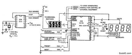
The circuit uses an ICM7213 precision one minute/one second timebase generator using a 4.1943 MHz crystal for generating pulses counted by an ICM7217B. The thumbwheel switches allow a starting time to be entered into the counter for a preset-countdown type timer, and allow the register to be set for compare functions. For instance, to make a 24-hour clock with BCD output the register can be preset with 2400 and the EQUAL output used to reset the counter. Note the 10 k resistor connected between the LOAD COUNTER terminal and ground. This resistor pulls the LOAD COUNTER input low when not loading, there by inhibiting the BCD output drivers. This resistor should be eliminated and SW4 replaced with an SPDT center-off switch if the BCD outputs are to be used. (View)
View full Circuit Diagram | Comments | Reading(2898)
EIGHT_CHANNEL_SEQUENTIAL
Published:2009/7/7 4:59:00 Author:May

Eight different analog inputs are sampled by National LF13508 multiplexor and converted into digital words for furtner processing. Maximum throughput rate of system is 2800 samples per second per channel. Output will settle to ±0.05mV in 1μs after hold command.- FET Data-book, National Semiconductor, Santa Clara, CA, 1977, p 5-77-5-78. (View)
View full Circuit Diagram | Comments | Reading(607)
VOLTAGE_TO__FREQUENCY_USING_IC_TIM_ERS
Published:2009/7/7 4:59:00 Author:May
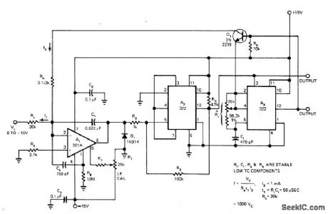
Two 322 IC timers and single 301A opamp provide all functions required for charge-balancing type of voltage-to-frequency converter, including integrator, level sensor or comparator, precision mono, and gated current source. Circuit accepts control voltage inputs of 0 to -10 V, corresponding to output pulse stream range of 0 to 10 kHz. Article describes operation in detail. R4, should be 4.7 megohms. Output pulses of comparator A3 trigger mono A2, which generates pulse having duration t1 that saturates Q1, to force reference current l2, into summing point of opamp integrator.-W.G. Jung, Take a Fresh Look at New IC Timer Applications, EDN Magazine, March 20, 1977, p 127-135. (View)
View full Circuit Diagram | Comments | Reading(1283)
ANALOG_TO_PULSE_WIDTH
Published:2009/7/7 4:53:00 Author:May
Stripped-down version of dual-slope A/D converter integrates input current constantly but switches reference current into integrator each time clock pulse occurs. Accuracy of 0.1% makes circuit suitable for use in digital voltmeter. Reference current is switched out of integrator when output voltage reaches +4.5V. With values shown, using 100 kilohms for R1, maximum input current is 80 μA and full-scale voltage is 8 V. Article includes timing diagram and design equations.-N. A. Robin, Analog-to-Pulse-Width Converter Yields 0.1% Accuracy, EDN Magazine, Nov. 1, 1970, p 42-43. (View)
View full Circuit Diagram | Comments | Reading(962)
RMS_TO_DC
Published:2009/7/7 4:51:00 Author:May
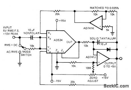
Single AD534 analog multiplier and two opamps compute RMS value of input signal as square root of sum of squares. Input is first squared at X2 and Y1 then time-averaged by integrator. Closing output loop back to X1 and Y2 completes square-rooting function. Crest factors up to 10 do not appreciably affect accuracy as long as input limits of multiplier are not exceeded. Accuracy is maintained up to 100 kHz. Article gives calibration procedure.-R. Frantz, Analog Multipliers-New IC Versions Manipulate Real-World Phenomena with Ease, EDN Magazine, Sept. 5, 1977, p 125-129. (View)
View full Circuit Diagram | Comments | Reading(1012)
| Pages:245/471 At 20241242243244245246247248249250251252253254255256257258259260Under 20 |
Circuit Categories
power supply circuit
Amplifier Circuit
Basic Circuit
LED and Light Circuit
Sensor Circuit
Signal Processing
Electrical Equipment Circuit
Control Circuit
Remote Control Circuit
A/D-D/A Converter Circuit
Audio Circuit
Measuring and Test Circuit
Communication Circuit
Computer-Related Circuit
555 Circuit
Automotive Circuit
Repairing Circuit