
Basic Circuit
Index 261
12_ns_CIRCUIT_BREAKER
Published:2009/7/6 5:28:00 Author:May

This circuit will turn off current in a load 12 ns after it exceeds a preset value. Under normal conditions the voltage across the 10 ohm shunt is smaller than the potential at the LT1016's negative input. This keeps Q1 off and Q2 receives bias, driving the load. When an overload occurs the current through the 10 ohm sense resistor begins to increase. When this current exceeds the preset value, the LT1016's outputs reverse.
This provides ideal turn-on drive for Q1 and it cuts off Q2 in 5 ns. The delay from the onset of excessive load current to complete shutdown is just 13 ns. Once the circuit has triggered, the LT1016 is held in its latched state by feedback from the non-inverting output. When the load fault has been cleared the pushbutton can be used to reset the circuit. (View)
View full Circuit Diagram | Comments | Reading(618)
HIGH_SPEED_ELECTRONIC_CIRCUIT_BREAKER
Published:2009/7/6 5:26:00 Author:May

This 115 Vac, electronic circuit breaker uses the low drive power, low on resistance and fast turn off of the TMOS MTM15N50. The trip point is adjustable, LED fault indication is provided and battery power provides complete circuit isolation.
The two circuit breaker terminals are across one leg of a full wave diode bridge consisting of D1-D4. Normally, Q1 is turned ON so that the circuit breaker looks like a very low resistance. One input to comparator U1 is a fraction of the internal battery voltage and the other input is the drop across zeners D6 and D7 and the voltage drop across R1. If excessive current is drawn, the voltage drop across R1 increases beyond the comparator threshold (determined by the setting of R6), U1 output goes low, Q1 turns OFF, and the circuit breaker opens. When this occurs, the LED fault indicator is illuminated. (View)
View full Circuit Diagram | Comments | Reading(1098)
SAMPLE_AND_HOLD_CIRCUIT
Published:2009/7/6 5:25:00 Author:May
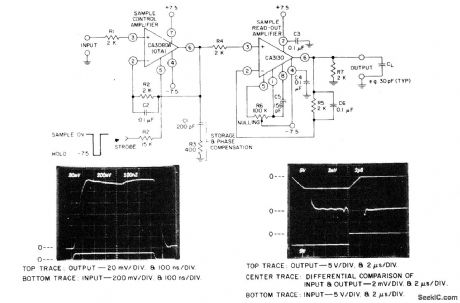
Circuit Notes
The circuit uses a CA3130 BiMOS op amp as the sample-readout amplifier for the storage (sample-holding) capacitor C1, and a CA3080A as the sample-control amplifler. Applications in linear systems to temporarily store analog data include DVM systems, industrial process-control, multiplex systems, and A-D converters. (View)
View full Circuit Diagram | Comments | Reading(747)
9_V_BATTERY_LIFE_EXTENDER
Published:2009/7/6 5:24:00 Author:May
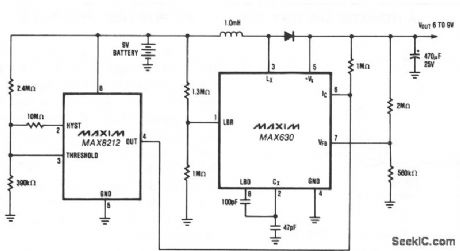
Circuit provides a minimum of 7 V until the 9-V battery voltage falls to less than 2 V. When the battery voltage is above 7 V, the MAX630's IC pin is low, putting it into the shutdown mode which draws only 10 nA. When the battery voltage falls to 7 V, the MAX8212 voltage detector's output increases. The MAX630 then maintains the output voltage at 7 V. The low battery detector (LBD) is used to decrease the oscillator frequency when the battery voltage falls to 3 V, thereby increasing the output current capability of the circuit. Note that this circuit, with or without the MAX8212, can be used to provide 5 V from 4 alkaline cells. The initial voltage is approximately 6 V, and the output is maintained at 5 V even when the battery voltage falls to less than 2 V. (View)
View full Circuit Diagram | Comments | Reading(660)
100_HZ_SQUARE_TRIANGLE
Published:2009/7/6 5:23:00 Author:May

Two-opamp oscillatordelivers ±13 V square waves and ±10V triangle waves simultaneously at 100 Hz for values shown. By scaling R1, R2, and C1, wide range of frequencies can be covered down to o.1z (increase R2 to 10 megohms for frequencies near lower limit). Square-wave rise time is about 1.5 μs and fall time 0.5 μs. Opamp A1 operates as integrator and A2 as Schmitt trigger.-R. S. Burwen, Triangular and Square Wave Generator Has Wide Range, EDN Magazine, Dec. 1, 1972, p 59. (View)
View full Circuit Diagram | Comments | Reading(728)
NICAD_BATTERY_PROTECTION_CIRCUIT
Published:2009/7/6 5:23:00 Author:May
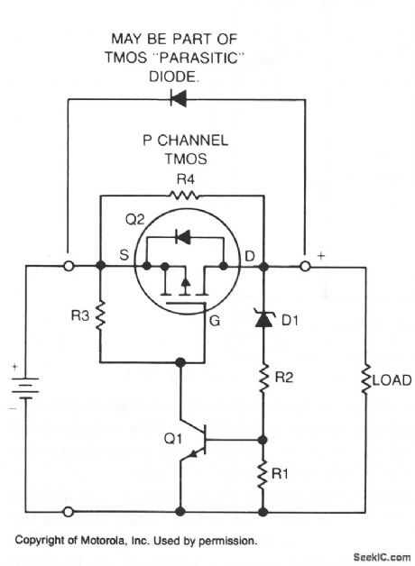
If a NiCad battery is discharged to a point at which the lowest capacity cell becomes fully discharged and reverses polarity, that cell will usually short internally and become unusable. To prevent this type of damage, this circuit detects a one-cell drop of 1.25 V and turns the load off before cell reversal can occur.
Low-current zener or other voltage sensor D1 and resistors R1 and R2 establish a reference level for transistor Q1. These resistors bias the zener to a few microamperes above its knee. Therefore, if battery voltage falls more than 1.25 V, Q1 turns off, turning off Q2, and disconnecting the load.After the load is disconnected, if the battery returns to nominal voltage, the high value of resistor shunting Q2 provides enough output voltage to reset the voltage sensor and tum Q2 back on. If desirable, shunt diode D2 or the parasitic diode of the TMOS device, if suitable, allows the battery to be charged from the load terminals.
The protection circuit presents a shunt current of only 10 mA at nominal battery voltage, which is low relative to the intemal leakage of the batteries. (View)
View full Circuit Diagram | Comments | Reading(861)
4W DC converter circuit composed of CW1524A
Published:2011/5/10 1:45:00 Author:Rebekka | Keyword: 4W DC converter

4W DC converter circuit composed of CW1524Ais shown as above. (View)
View full Circuit Diagram | Comments | Reading(598)
PROGRAMMABLE_ACTIVE_FILTERS
Published:2009/7/6 5:16:00 Author:May

This is a second-order, low-pass filter with programmable cutoff frequency. This circuit should be driven from a low-source impedance since there are paths from the output to the input through the unse-lected networks. Virtually any filter function which can be constructed with a conventional op amp can be made programmable with the HA-2400.
A useful variation would be to wire one channel as a unity gain amplifier, so that one could select the unfiltered signal, or the same signal filtered in various manners. These could be cascaded to provide a wide variety of programmable filter functions. (View)
View full Circuit Diagram | Comments | Reading(811)
LOW_BATTERY_WARNING
Published:2009/7/6 5:07:00 Author:May

A voltage divider consisting of R1, R2, and R3 is used to set the input reference voltage below which the batteries are to be replaced. That reference voltage, at point A, is varied by R1. With the voltage divider shown in Fig. 9-7, a range of 2 to 3.5 V is possible. When the battery voltage drops below that at point A, the output of IC1a, 1/4 of a LM339 quad comparator, switches from high to low. That triggers IC1b, which is configured as an astable multivibrator. Feedback resistors R6 and R7, coupled with capacitor C1,determine the time constant of the multiibrator. The output from IC1b is connected to LED1 through dropping resistor R8. With the circuit values as shown, the LED will flash at a rate of 3 Hz.Although this circuit was designed specifically to monitor RAM back-up batteries, it can of course be modified for use in just about any application where the condition of a battery must be found. (View)
View full Circuit Diagram | Comments | Reading(1213)
SINGLE_TIMER_IC_PROVIDES_SQUARE_WAVE_TONE_BURSTS
Published:2009/7/6 5:01:00 Author:May
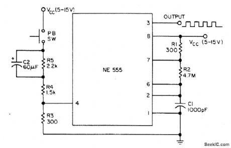
The tone-burst generator gives a 50-ms burst of 1.5 kHz square waves with each operation of the pushbutton and can source or sink 200 mA. (View)
View full Circuit Diagram | Comments | Reading(548)
05_25_kHz_TRIANGLE
Published:2009/7/6 5:01:00 Author:May

Diode bridge and FET form constant-current source charging c1,to make voltage across c1 change at linear rate as required for triangle output across c1. Frequenεy can be adjusted from 500 Hz to above 20 kHz with constant output amρlitude, by means of R1 Short -term stabilityis better than1 partin l0.000 Since the same R and C are used to generate both sections of the waveform,ρositive and negative slopes are identical,Diodesare HP 5082-2810.-G. R. Begaulg, oρ AmρMakes Variable-Frequency Tliangular Wave Generator,EDN Magazine, Sept 15,1972,ρ 42-43.
(View)
View full Circuit Diagram | Comments | Reading(733)
BRIDGE_CIRCUIT
Published:2009/7/6 4:43:00 Author:May
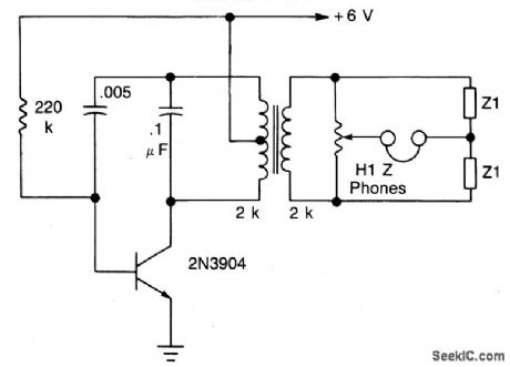
The transistor is connected as an audio oscillator, using an audio transformer in the collector. The secondary goes to a linear pot. The ratio between the two parts of the pot from the slider is proportional to the values of Z1 and Z2 when no signal is heard in the phones. (View)
View full Circuit Diagram | Comments | Reading(1470)
FIBER_OPTIC_LINK
Published:2009/7/6 4:40:00 Author:May
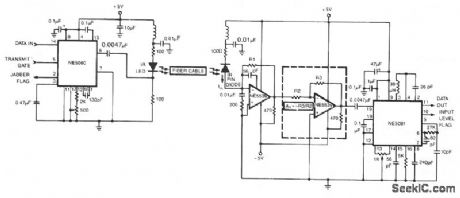
The circuit shows a simplex fiber link between the NE5080 transmitter and the NE5081 receiver. The components shown are for a center frequency of 5 MHz, although this frequency can be increased to 20 MHz with proper selection of external component values. The NE5539 has a 530-MHz unity gain bandwidth which could limit maximum operating frequencies in some systems. Since the NE5081 can adequately accept signals below 10 mV at 5-MHz carrier, the gain stage within the dashed lines can be eliminated if the attenuation in the link is low. If the gain stage is used, be mindful of the bandwidth tradeoff at higher gains. Refer to the NE5539 data sheet for details. (View)
View full Circuit Diagram | Comments | Reading(2288)
AC_BRIDGE
Published:2009/7/6 4:38:00 Author:May
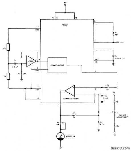
The circuit provides a simple and cost-effective solution to matching resistors and capacitors. Impedances ZR and Zx form a half-bridge, while OSC and OSC excite the bridge differentially. The external op amp is a FET input amplifier (LF356) with very low input bias current on the order of 30 pA (typical). C1 allows ac coupling by blocking the dc common mode voltage from the bridge, while RI biases the output of LF356 to 0 V at dc. Use of FET input op amp insures that dc offset due to bias current through R1 is negligible. Ac output of the demodulator is filtered via the uncommitted amp to provide dc voltage for the meter. The 10 k potentiometer, R5, limits the current into the meter to a safe level. Calibration begins by placing equal impedances at ZR and ZX, and the system offset is nulled by the offset adjust circuit so that Pin 1 is at 0 V. Next, known values are placed at Zx and the meter deviations are calibrated. The bridge is now ready to measure an unknown impedance at Zx with ±0.05% accuracy or better. (View)
View full Circuit Diagram | Comments | Reading(861)
Simple_Z80_interface_for_A_D_converter
Published:2009/7/23 2:04:00 Author:Jessie
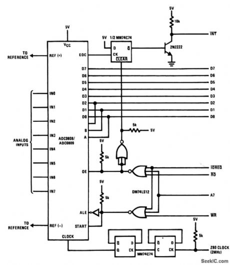
This circuit shows a simple Z80 interface for the ADC0808/0809, The inter-face is similar to that of Fig. 6-20, except that the interrupt is flip-flop closer to the 6800 (because of the Z80 INT is active low as in the 6800, but the INS8080 is active high). (View)
View full Circuit Diagram | Comments | Reading(423)
SQUARE_TRIANGLE_AF
Published:2009/7/6 4:13:00 Author:May
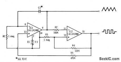
Two sections of LM3900 quad opamp are connected to generate dua-polarity triangle-and square-wave AF outputs while oρerating from single supply, byusing current mirror circuit at noninverting input Value used for C1 determines frequency and pulse width;frequency ranges from 0.5 Hz with 1 μF to 3800 Hz with 0.0001 μF and 21 kHzwith C1 omitted, Pulse-width rangeis 35μs without C1 to 1.6 s with 1 μF.-F.M Mims,″Integrated Circuit Projects,Vol.5,″Radio Shack,Fort Worth,TX,1977、2nd Ed. p 57-63 (View)
View full Circuit Diagram | Comments | Reading(689)
LOW_POWER_RS_232C_DRIVER
Published:2009/7/6 4:05:00 Author:May
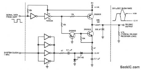
This circuit draws only 4 mA from a 5-V supply while driving a standard RS-232C receiver. The system clock drives a dc-dc converter that produces -3.4 V. The frequency can range from 0.5 to 8 MHz, but a range of 0.5 to 1 MHz will minimize power dissipation. The circuit output withstands direct shorts to ground or to either of the supplies (±12 V max). In place of the 74HC04 high-speed CMOS driver shown, you may want to substitute miscellaneous spare gates; one noninverting buffer, for example, can replace the two inverting types that receive the UART signal. (View)
View full Circuit Diagram | Comments | Reading(526)
LINE_SYNCHRONIZED_DRIVER
Published:2009/7/6 3:59:00 Author:May
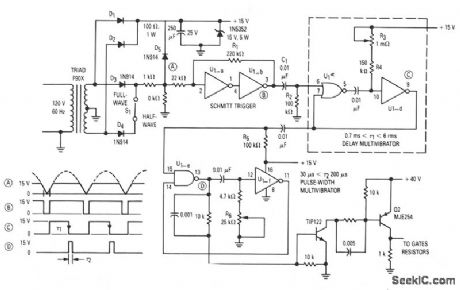
The gate drive that phase controls the four parallel SCRs is accomplished with complementary MOS hex gate MC14572 and two bipolar transistors. This adjustable line-synchronized driver permits SCR conduction from near zero to 180 degrees. A Schmitt trigger clocks a delay monostable multivibrator that is followed by a pulse-width monostable multivibrator. Line synchronization is achieved through the half-wave section of the secondary winding of the full-wave, center-tapped transformer. This winding also supplies power to the circuit through rectifiers D1 and D2. (View)
View full Circuit Diagram | Comments | Reading(2198)
PRACTICAL_CURRENT-LIMITING_COIL_DRIVER
Published:2009/7/6 3:54:00 Author:May
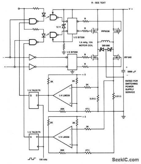
The p-channel devices are switched off by current sensors when the coil current reaches 10 A. The operation is similar to that of a switching-type power supply. The Schottky diodes and resistors are for spike protection. (View)
View full Circuit Diagram | Comments | Reading(484)
VOLTAGE_TUNED_WITH_10;1_FREQUENCY_RANGE
Published:2009/7/6 3:49:00 Author:May

Exar XR-S200 PLL IC is connected to generate basic periodic square or sawtooth waveform. Multiplier section, used as linear differential amplifier, converts diffetential sawtooth input waveform to triangle wave. 5K pot connected between pins 8 and 9 rounds peaks of triangle to give low-distortion sine wave with less than 2% total harmonic distortion. Output frequency can be swept or frequency-moduiated by applying proper analog control input.For linear frequency modulation with less than 10% deviation, modulation is applied between pins 23 and 24. For larger deviations, negativegoing sweep voltage Vs is applied to pin 18 as shown. Digital control input pins 15 and 16 can be used for FSK applications; if this is not desired, pins are disabled by connecting to ground through current-limiting resistor.- Phase-Locked Loop Data Book, Exar Integrated Systems, Sunnyvale, CA, 1978, p 9-16. (View)
View full Circuit Diagram | Comments | Reading(483)
| Pages:261/471 At 20261262263264265266267268269270271272273274275276277278279280Under 20 |
Circuit Categories
power supply circuit
Amplifier Circuit
Basic Circuit
LED and Light Circuit
Sensor Circuit
Signal Processing
Electrical Equipment Circuit
Control Circuit
Remote Control Circuit
A/D-D/A Converter Circuit
Audio Circuit
Measuring and Test Circuit
Communication Circuit
Computer-Related Circuit
555 Circuit
Automotive Circuit
Repairing Circuit