
Basic Circuit
Index 264
THREE_TIME_BASE_WlNDOWS
Published:2009/7/6 2:48:00 Author:May
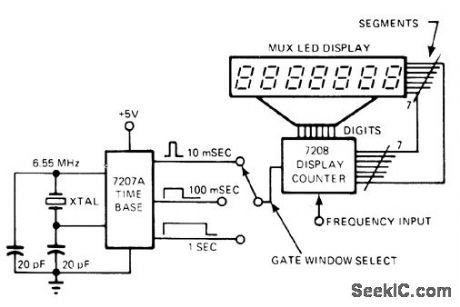
Intersil 7207A crystal-controlled timer generates precision gate windows of10 ms,100 ms, and 1 s for use as time bases, calibration markers, or gate timerns for frequency counters such as 7208.-B.O'Neil, IC Timers-the Old Reliable 555 Has Company, EDN Magazine, Sept. 5, 1977, p 89-93.
(View)
View full Circuit Diagram | Comments | Reading(765)
300_MHz_PRESCALER_1
Published:2009/7/6 2:46:00 Author:May
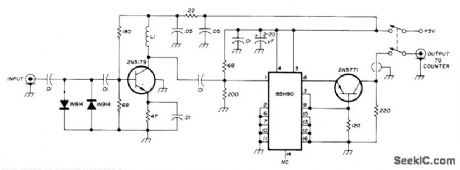
Divides inputfrequency by 10 for extending range of digital frequency counter up to prescaler limit of 300 MHz. Reading of counter must be multiplied by 10. Article also gives circuits of high-resolution counters using CMOS TTL devices.-H. E. Harris, Simplifying the Digital Frequency Counter,Raido,Feb 1978,p 22-25. (View)
View full Circuit Diagram | Comments | Reading(3788)
Bipolar_offset_true_zero_D_A_converter
Published:2009/7/23 21:48:00 Author:Jessie

This circuit shows a DAC/op-amp combination that is bipolar-offset (true zero) operation. Full-scale adjustment can be in Fig. 6-39B. (View)
View full Circuit Diagram | Comments | Reading(534)
PREAMP_FOR_CMOS_LOGIC
Published:2009/7/6 2:44:00 Author:May

Combination of CA3130 and CD4010 ICs provides broad fre-quency response at very low power levels, as required for driving frequency counter. Diodes protect input from overvoltage. Amplifier offset control pot is used as trigger level control. Input sensitivity of amplifier/trigger combination is 50 mV P-P from 1 Hz to 1 MHz.-R. Tenny, Counter Pre-Amp Matches CMOS Logic Capability, EDN Magazine, Sept. 20, 1976, p 114 and 116. (View)
View full Circuit Diagram | Comments | Reading(1429)
BASIC_SQUAREN_TRIANGLE
Published:2009/7/6 2:43:00 Author:May

Requires only two sections of LM324 quad differential-input opamp to provide choice of triangle or squarewave outputs at frequency determined by values of components. Supply voltage range is 3-32 V.- Quad Low Power Operational Amplifiers, Motorola, Phoenix,AZ, 1978, DS 9339 R1.
(View)
View full Circuit Diagram | Comments | Reading(2371)
10_Hz_TO_2_MHz
Published:2009/7/6 2:41:00 Author:May
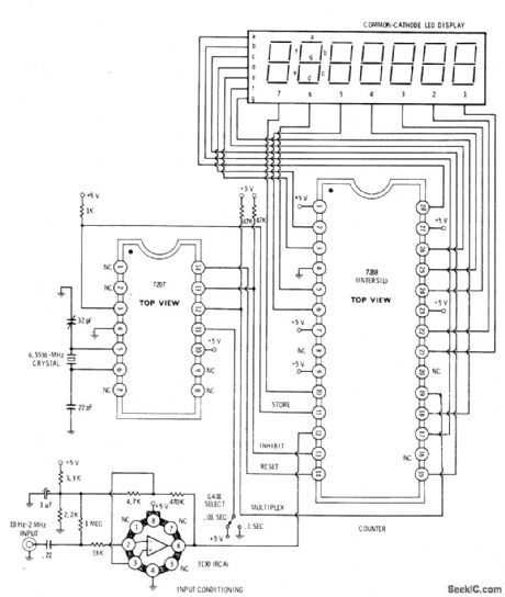
Seven-decade Intersil 7208 latched and multiplexed frequency counter with direct digit and display drive obtains timing waveform from 7207 IC which dlvides6,5536-MHz crystal oscillator output by 212 to produce 1600-Hz square, ave for multiplexing counter and display. Square wave is further divided to produce 0.1-sand 0.01-s counting gates along with reset and update commands. RCA 3130 opamp is used for conditioning of input signaL-D. Lancaster, CMOS Cookbook, Howard W. Sams, Indianapolis, IN, 1977, p 380-382.
(View)
View full Circuit Diagram | Comments | Reading(2408)
10_1_SCALER
Published:2009/7/6 2:40:00 Author:May
Used to increase range of frequency counter. Sensitivity is 20 mV at 175 MHz, 40 mV at 220 MHz, and 90 mV at 250 MHz.Fairchild IC is used. Simple L-section filter at output rolls off frequencies above 30 MHz, allowing sealer to be used up to 250 MHz without erroneous counting of second or third harmonics of squarewave output of scaler if counter in use will respond to 60 MHz or more.-E. Guerri, Frequency Pre-Scaler, Ham Radio, Feb. 1973, p 57. (View)
View full Circuit Diagram | Comments | Reading(1414)
FSK_SINE_SQUARE_TRIANGLE_GENERATOR
Published:2009/7/6 2:40:00 Author:May
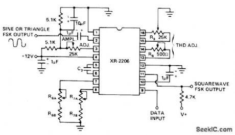
Exar XR-2206 modulator-demodulator (modem) is connected as function generator providing high-purity sinusoidal output along with triangle and square outputs, for FSK applications. Circuit has excellent frequency stability along with TTL and CMOS compatibility.Total harmonic distortion in 3 V P-P sine output is about 2.5% untrimmed, but can be trimmed to 0.5%. High-level data inputsignal selects frequency of 1/R6C3 Hz, while low-level input selects 1/R7C3 Hz. For optimum stability,R6 and R7 should be in range of 10K to 100K. Adiust R8 and R9 for minimum distortion.- Phase-Locked Loop Data Book, Exar Integrated Systems, Sunnyvale, CA, 1978, p 57-61. (View)
View full Circuit Diagram | Comments | Reading(6934)
SCALER_FOR_CB
Published:2009/7/6 2:35:00 Author:May


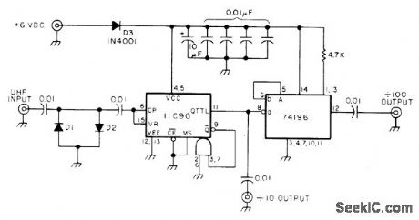
Low-cost prescaler for low-range frequency counter permits accurate monitoring of 450-MHz CB transceiver. Fairchild 11C90 decade counter gives division by 10 for counters covering up to 45 MHz. For lower-range counter, add 74196 TTL decade counter as shown to give total division by 100 for conversion to 4.5-MHz output. D1 and D2 should be fast-switching diodes such as 1N914 or 1N4148.Keep input signal under 1 V to avoid damaging 11C90. Will operate from 5-V supply or four D cells.-P. A. Stark, 500 MHz Scaler, 73 Magazine, Oct. 1976, p 62-63. (View)
View full Circuit Diagram | Comments | Reading(4243)
Basic_D_A_converter_configurations
Published:2009/7/23 21:47:00 Author:Jessie
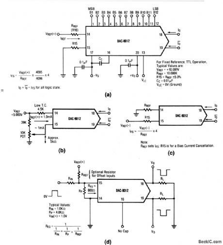
These circuits show various configurations for a DAC-6012 connected as a D/A converter for stand-alone operation. Figure 6-39A shows basic positive-reference operation. Figure 6-39B shows recommended full-scale adjustment circuit. Figure 6-39C shows basic negative-reference operation. Figure 6-39D shows pulsed-reference operation. (View)
View full Circuit Diagram | Comments | Reading(488)
Analog_multiplier_divider
Published:2009/7/23 21:47:00 Author:Jessie
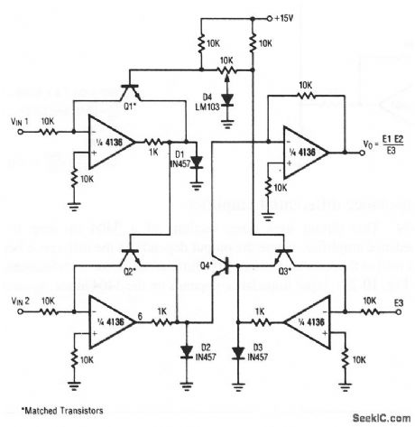
This circuit uses all four sections of a 4136 to form a circuit that both multiplies and divides (simultaneously if required). Virtually any pnp transistors can be used for Q1 through Q4, provided that the transistors are matched. The accuracy of the circuit multiplication and division depends on transistor matching. (View)
View full Circuit Diagram | Comments | Reading(816)
4O_1_SCALER_FOR_1200_MHz
Published:2009/7/6 2:33:00 Author:May
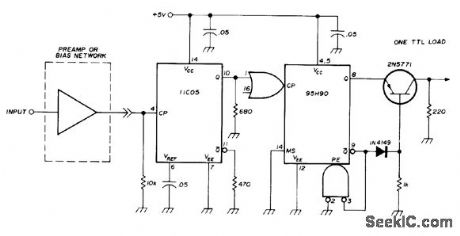
Uses Fairchild 11C05 divide-by 4 counter and 95H90 decade divider. Unused CP input is tied to ground. Transistor translates ECL level to TTL for driving one unit load. Operatesfrom single regulated power supply. Input may be AC or DC coupled so either input amplifier or simple bias network (also given in article) may be used. 10K resistor from pin 4 to ground eliminates noise triggering in middle frequency ranges.-D. Schmieskors, 1200-MHz Frequency Scalers, Ham Fladio, Feb.1975, p 38-40.
(View)
View full Circuit Diagram | Comments | Reading(801)
2500_FREQUENCIES_WITH_SYNCHRONIZA_TION
Published:2009/7/6 2:32:00 Author:May
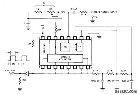
EXAR XR-2240 programmable timer/ counter containing 8-bit programmable binary counter and stable time-base oscillator can generate over 2500 discrete frequencies from single input reference frequency. Circuit simultaneously multiplies input frequency by factor M and divides by N + 1, where M and N are adjustable integer values. Output frequency Fo is equal to input frequency FR multiplied by M/(1 + N). M and N can be externally adjusted over broad range, with M between 1 and 10 and N between 1 and 255. Multiplication factor M is obtained by locking on harmonics of reference.Division factor N is determined by preprogrammed count in binary counter section, established by wiring appropriate pins 1-8 to output bus. Input reference is 3 V P-P pulse train with pulse duration ranging from 30% to 80% of time-base period T. R1 determines value of M. C is in range of 0.005 to 0.1 μF, and R is between 1K and1 megohm for maximum output frequency of about 200 kHz. With M = 5 and N = 2, 100-Hz clock synchronized to 60-Hz line frequency is obtained.- Timer Data Book, Exar Integrated Systems, Sunnyvale, GA, 1978, p 31-32. (View)
View full Circuit Diagram | Comments | Reading(909)
INPUT_BUFFER_FOR_100_MHz_COUNTER
Published:2009/7/6 2:31:00 Author:May

Can be used with 500-ohm probe for wide range of high-frequency input signal levels and waveforms, as part of frequency counter using standard emitter-coupled logic. Opamps used have 50-ohm input impedance. 450-ohm resistor in series with coax gives 10:1 attenuation factor (80 mV at amplifier input when measuring 800-mV ECL swing).-W. R. Blood, Jr., Measure Frequency and Propagation Delay with High Speed MECL Circuits, Motorola, Phoenix, AZ, 1972, AN-586, p 3. (View)
View full Circuit Diagram | Comments | Reading(787)
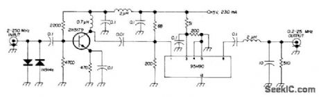
500_MHz_WITH_100_Hz_RESOLUTION
Published:2009/7/6 2:25:00 Author:May

Circuit provides separate 0-50 MHz preamp Q1-Q7 and 50-500 MHz prescaler for Intersil IC M7207A 7-digit CMOS frequency counter. 500-MHz prescaler uses Fairchild 11C90 that drives TTL directly, with 2N5179 transistor as preamp. L1 and output capacitance of 2N5179 form low-Q resonant circuit. U3 is 50-MHz presealer for both preamps. Crystal frequency is 5.242880 MHz. 5-V regulators are MC7805, and 12-V regulator is MC7812. Article covers construction and adjustment.-J. H. Bordelon, Simple Front-Ends for a 500-MHz Frequency Counter, Ham Radio, Feb. 1978, p 30-33.
(View)
View full Circuit Diagram | Comments | Reading(5133)
Low_cost_supervisory_circuit_with_battery_backup_30_V_33_V
Published:2009/7/23 21:38:00 Author:Jessie

Figures 1-40 and 1-41 show a typical application circuit and pin configuration, respectively, for the MAXTO4T/S/R. The ICs are similar to that described for Figs.1-J through 1-M, but with generally lower cost, and for use with 3.0-V/3.3-V systems. The ICs have a 200-ms reset time delay, 50-μA quiescent current, 50-nA quiescent with battery backup, and a 1.25-V threshold detector for power-fail warning, low-battery detection, or for monitoring a supply other than 3.0 V or 3.3 V. The T, S, and R versions have different threshold levels, as shown in Fig. 1-42. MAXIM NEW RE[,EASES DATA Book, 1994, p 5-43. (View)
View full Circuit Diagram | Comments | Reading(686)
0_25_V_WITH_FOLDBACK_CURRENT_LIMITING
Published:2009/7/6 2:24:00 Author:May
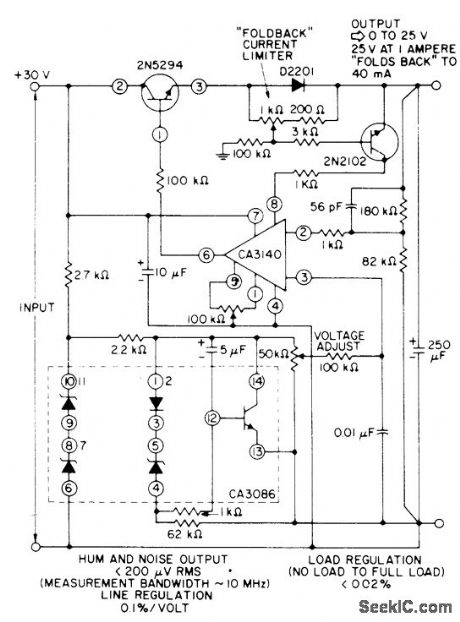
When D2201 diode senses load current of 1 A at maximum regulated output of 25V,2N2102 current-sensing transistor provides foldback of output current to 40 mA. Arrangement permits use of 2N5294 transistoras series-pass element,using only small heatsink. High-impedance reference-voltage divider across 30-V supply serves CA3140 connected as noninverting power opamp.- Linear Integrated Circuits and MOS/FET's, RCA Solid State Division, Somerville, NJ, 1977, p 248-257. (View)
View full Circuit Diagram | Comments | Reading(1432)
12V_AT_20A
Published:2009/7/6 2:23:00 Author:May
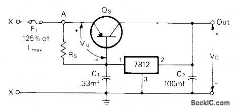
Regulator conducts and regulates until current demand is such that IR drop across RS is sufficient to overcome base-emitter junction potential of switch transistor QS, which is two 2N174 germanium transistors in parallel. Use 2 ohms for RS. QS is then turned on, with current/voltage regulation to its base controlled by regulator. Input voltage of 7812 regulatorshould be 2 V more than desired output voltage.
Article gives three different rectifier circuits suitable for use with regulator.-A. M. Clarke,Regulated 200 Watt-12 Volt D.C. Power Supply, CQ, Oct. 1975, p 28-30 and 78-79. (View)
View full Circuit Diagram | Comments | Reading(1907)
PARALLELING_REGU_LATORS
Published:2009/7/6 2:23:00 Author:May
Current-sharing problem is overcome without sacrificing ripple rejection or load regulation, by using bottom regulator as control device that supplies most of load current until current through this regulator reaches about 1.3 A. At this point Q1 turns on and raises output voltage of other regulators to supply additional load current de-mands. Circuit shown will supply up to 6A for minimum input voltage of 8V. For optimum regulation, minimum load current should be 1 A.-C. T. Nelson, Power Distribution and Regulation Can Be Simple, Cheap and Rugged, EDN Magazine, Feb. 20, 1973, p 52-58. (View)
View full Circuit Diagram | Comments | Reading(449)
AUTOMOBILE_LOCATER
Published:2009/7/6 2:22:00 Author:May

This locater is made up of two parts. The first is an rf oscillator, whose circuit is shown in Fig. 8-4a.The second is a sensitive receiver shown in Fig. 8-4b. The heart of the oscillator is a 555 timer IC. Tank circuit C2 and L1 is used to tune the transmitter. The antenna is coupled to the transmitter through C3. A telescopic antenna or a length of hookup wire will work quite well. At the receiver, the incoming signal is tuned by C5 and L2 before being passed on to the 741 IC. The five LEDs are used to indicate signal strength, they light up in order (1 to 5) as the signal gets stronger.
After the devices are built, the receiver and transmitter will need to be tuned. Tune the transmitter until all of the receiver's LEDs light. Separate the receiver and the transmitter-the farther apart they are the better-and adjust R4 until you get a maximum strength reading only when the receiver's antenna is pointed directly at the transmitter. Place the transmitter on the dashboard and completely extend the antenna. To find your car, just extend the telescope antenna to its full length and hold it parallel to the ground. Point the antenna to your far left, then swing it to your far right. Do that until you find in which direction the strongest signal lies, as indicated by the LEDs. The antenna will be pointing at your car. (View)
View full Circuit Diagram | Comments | Reading(744)
| Pages:264/471 At 20261262263264265266267268269270271272273274275276277278279280Under 20 |
Circuit Categories
power supply circuit
Amplifier Circuit
Basic Circuit
LED and Light Circuit
Sensor Circuit
Signal Processing
Electrical Equipment Circuit
Control Circuit
Remote Control Circuit
A/D-D/A Converter Circuit
Audio Circuit
Measuring and Test Circuit
Communication Circuit
Computer-Related Circuit
555 Circuit
Automotive Circuit
Repairing Circuit