
Basic Circuit
Index 272
1_kHz_WIEN_BRIDGE
Published:2009/7/5 22:34:00 Author:May
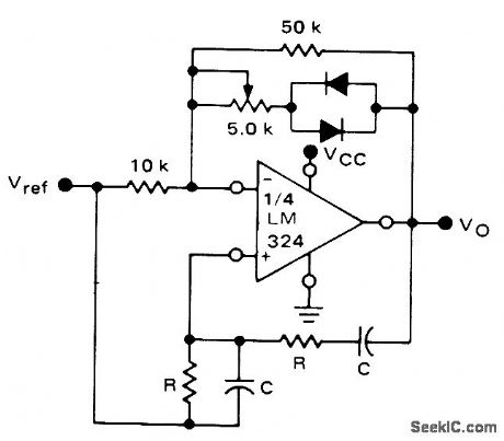
Simple circuit uses only one section of LM324 quad opamp having true differential inputs. Supply voltage range is 3-32 V. Reference voltage is half of supply voltage.Values of R and C determine frequency accord-ing to equation f = 1/6.28RC. For 16K and 0.01 μF, frequency is 1 kHz. Diode types are not criticaL- Quad Low Power Operational Amplifiers, Motorola, Phoenix, AZ, 1978, DS 9339 R1. (View)
View full Circuit Diagram | Comments | Reading(932)
ISOLATION_AND_ZERO_VOLTAGE_SWITCHING_LOGIC
Published:2009/7/5 22:33:00 Author:May

These two simple circuits provide zero voltage switching. They can be used with full wave bridges or in antiparallel to provide full wave control and are normally used to trigger power thyristors. If an input signal is present during the time the ac voltage is between 0 to 7 V, the SCR will turn on. But, if the ac voltage has risen above this range and the input signal is then applied, the transistor, Q1, will be biased to the on state and will hold the SCR and, consequently, the relay off until the next zero crossing. (View)
View full Circuit Diagram | Comments | Reading(1324)
Fronting Prescale Integrated Circuit of TD6134AF Dual Mode
Published:2011/7/22 22:51:00 Author:Michel | Keyword: Dual Mode, Fronting Prescale, Integrated Circuit


TD6134AF integrated circuit provides fronting prescaler used in low voltage power supply type digital tuned system and the working frequency maximum is 250 MHz.
First,TD6134AF Inside Circuit Block Diagram and Pins Functions
Inside circuit block diagram of TD6134AF intergrated circuit is shown as picture 1.This IC adopts 8 feet DIP structure and its pins functions and data of the intergrated circuit are shown as table.
Inside Circuit Block Diagram of TD6134AF Intergrated Circuit
Second,Typical Application Circuit of TD6134AF
The typical application circuit of TD6134AF intergrated block is shown as picture 2.
Third,TD6134AF Main Functions Because the FM frequency signal is 108 MHz and a 10.7 MHz intermediate frequency is added and the highest vibration FM is 118.7MHz.
(View)
View full Circuit Diagram | Comments | Reading(684)
HIGH_SENSITIVITY,NORMALLY_OPEN,TWO_TERMINAL,ZERO_VOLTAGE_SWITCHING,HALF_WAVE_CONTACT_CIRCUIT
Published:2009/7/5 22:30:00 Author:May
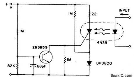
The SCR coupler circuit provides higher sensitivity toinput signals as illustrated.This allows the lower cost 4N39(H11C3)to be used with the>7 mA drive currentssupplied by the input circuit. (View)
View full Circuit Diagram | Comments | Reading(544)
1_kHz_FAST_START_GATED
Published:2009/7/5 22:30:00 Author:May
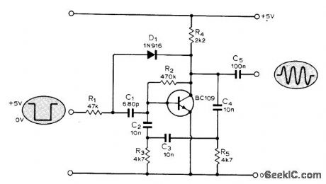
Circuit is conventional phase-shift oscillator in which frequency is determined by C2. C3. C4. R5. R3. and input impedance of transistor. When input is +5 V, almost 100 % negative feedback blocks oscillator. When input drops to0 V. D1 is reversebiased and negative feedback is removed. At same time, edge of input pulse is applied to transistor base to kick off oscillator on its first half-cycle, which is always in phase with falling edge of input signal.-G. F. Butcher. Gated Oscillator with Rapid Start. Wireless World. Aug. 1974. p 272. (View)
View full Circuit Diagram | Comments | Reading(624)
FLAME_DETECTOR_DRIVES_TTL_LOAD
Published:2009/7/5 22:29:00 Author:May
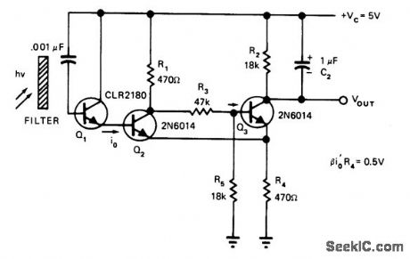
Sensor is silicon Darlington phototransistor Q1 having peak response near infrared bands. Filter is re quired to reduce interference from visible light sources. Circuit is sensitive enough to pick up hydrogen flames that emit no visible light. Article describes operation of circuit and gives design equations. Output can go directly to input port of microprocessor.-A. Ames, This Flame Detector Interfaces Directly to a μP, EDN Magazine, Oct. 20, 1976, p 122 and 124. (View)
View full Circuit Diagram | Comments | Reading(1155)
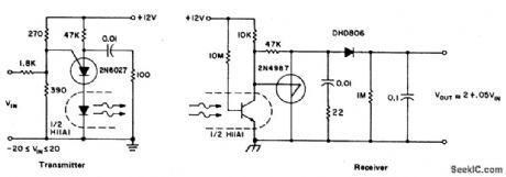
RECEIVER_FOR_REMOTE_TERMINAL
Published:2009/7/5 22:29:00 Author:May

National DM8820 receiver at computer location is connected by twisted-pair line to remote terminal.NE555 oscillator is set at 1760 Hz within 1% with aid of frequency counter, to match corresponding clock in remote terminal. Serial bits coming over line are converted to parallel bits for computer by AY-5-1013 UART. Article gives circuit for remote terminal and covers operation in detail-S. Ciarcia, Come Upstairs and Be Respectable, BYTE, May 1977, p 50-54. (View)
View full Circuit Diagram | Comments | Reading(943)
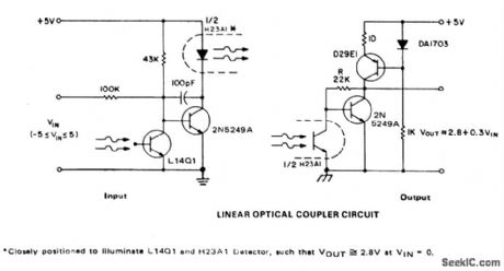
LINEAR_ANALOG_COUPLER
Published:2009/7/5 22:29:00 Author:May
The minimum parts count version of this system provides isolated, linear signal transfer useful at shorter distances or with an optocoupler for linear information transfer.
Although the output is low level and cannot be loaded significantly without harming accuracy, a single LC. operational or instrumentation amplifier can supply both the lin-ear gain and buffering for use with a variety of loads. (View)
View full Circuit Diagram | Comments | Reading(585)
Pincushion correction circuit
Published:2011/7/26 2:59:00 Author:Christina | Keyword: Pincushion correction circuit
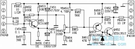
The field sawtooth wave voltage adds to the pincushion correction circuit through the pin-4 of P404, the integral circuit is composed of the R455, C454 and R457, this integral circuit integrates the field sawtooth wave to form the convex parabolic wave voltage, and this voltage adds to the B pole of the parabolic wave plastic amplification tube Q451 to be amplified and reformed, and the C pole outputs the 9V (peak-peak value) concave parabolic wave voltage, this voltage adds to the B pole of the composited tube which is composed of the Q453 and Q452 through the horizontal amplitude adjustment and left & right pincushion distortion adjustment network, so the C pole of the Q452 outputs the 12.5V (peak-peak value) parabolic wave voltage.
(View)
View full Circuit Diagram | Comments | Reading(608)
1_9_kHz_PLL_1
Published:2009/7/5 22:28:00 Author:May

Frequency multiplication is achieved with Signetics NE564 PLL by inserting counter in Ioop between VCO and phase comparator. VCO is then running at multiple of input frequency determined by counter; with connections and values shown, multiplication factor for 60-Hz input signal is 100, giving 6-kHz square-wave output.-''SigneticsAnalog Data Manual,''Signetics, sunnyvale,CA,1977,p 830-831 (View)
View full Circuit Diagram | Comments | Reading(1614)
SIMPLE_AC_RELAY_USING_TWO_PHOTON_COUPLERS
Published:2009/7/5 22:27:00 Author:May
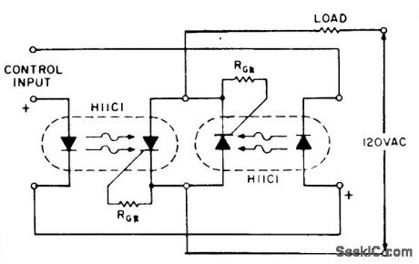
If load current requirements are relatively low (i.e. maximum forward rms current 500 mA), an ac solid state relay can be constructed quite simply by the connection of two H11C optically coupled SCRs in a back-to-back configuration as illustrated. (View)
View full Circuit Diagram | Comments | Reading(550)
LINEAR_AC_ANALOG_COUPLER
Published:2009/7/5 22:27:00 Author:May
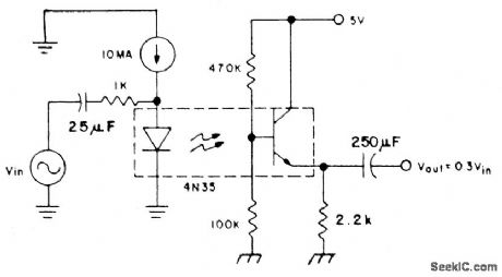
With the coupler biased in the linear region by the 10 mA dc bias on the IRED and the voltage divider on the phototransistor base, photodiode current flows out of the base into the voltage divider, producing an ac voltage proportional to the ac current in the IRED. The transistor is biased as an emitter follower and requires less than 10% of the photodiode current to produce the low impedance ac output across the emitter resistor. Note that the H11AV1 may be substituted for the 4N35 to provide VDE line voltage rated isolation of less than 0.5 pF. (View)
View full Circuit Diagram | Comments | Reading(1987)
MCS-51 microcontroller circuit remote controlled by TC9148
Published:2011/7/26 3:32:00 Author:Christina | Keyword: microcontroller circuit, remote controlled
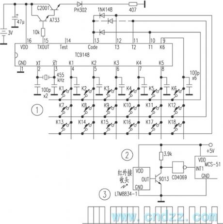
The TC9148 is designed as the CMOS low power consumption infrared remote control launch special IC, and it is usually used with the TC9149/TC9150 infrared remote control receiver IC to control the household appliances.
The principle of the transmitter is as shown in figure 1. The static power consumption of the TC9148 is very low, you need not to set the power switch. The readers also can use the remote controller product that is made with the TC9148. The author codes the first 3 bits of 101 , so the second diode does not need to connect. The principle of the receiver is simple, as the figure 2 shows. The infrared receiver uses the finished product, it sends the signal to the INT1 port of the single-chip microcomputer.
(View)
View full Circuit Diagram | Comments | Reading(2289)
DC_LINEAR_COUPLER
Published:2009/7/5 22:26:00 Author:May
The accuracy of direct linear coupling of analog current signals via an optocoupler is determined by the coupler linearity and its temperature coefficient. Use of an additional cdupler for feedback can provide linearity only if the two couplers are perfectly matched and identically biased. These are not practical constraints in most equipment designs and indicate the need for a different design approach. One of the most successful solutions to this problem can, be illustrated by using a H23 emitter-detector pair and a L14H4, The H23 detector and L14H4 are placed so both are illuminated by the H23 IRED emitter.Ideally, the circuit is mechanically designed such that the H23 emitter may be positioned to provide VOUT=2.8V when VIN=0, thereby insuring collector current matching in the detectors. Then all three devices are locked in position relative to each other.Otherwise, R may be adjusted to provide the proper null level, although temperature tracking should prove worse when R is adjusted. Note that the input bias is dependent on power supply voltage, although the output is relatively independent of supply variations.Testing indicated linearity was better than could be resolved, due to alignment motion caused by using plastic tape to lock positions. The concept of feedback control of IRED power output is useful for both information transmission and sensing circuitry. (View)
View full Circuit Diagram | Comments | Reading(871)
Remote control code launching, decoding receiving circuit composed of the F03/J02B
Published:2011/8/1 1:36:00 Author:Christina | Keyword: Remote control code, launching, decoding, receiving circuit
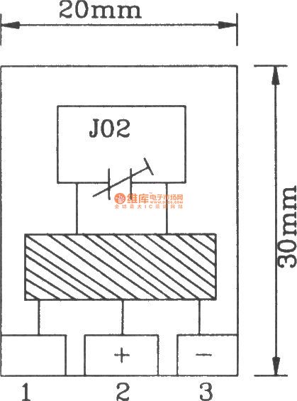
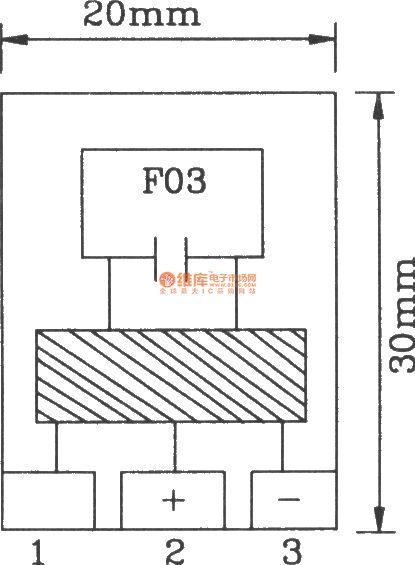
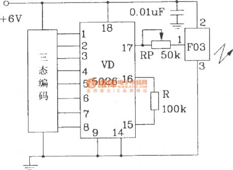

The F03/J02 FM launch/receiving module has the features of small volume, few external components, low voltage power consumption, high efficiency and stable performance. And the module uses the printing plant coil and it operates at the micro-wave side, so the operating frequency is stable and the interference is little, the transmission distance is far, and there is no need to use the external antenna to achieve the effective transmitter / receiver distance. You can use the F03/J02 in the remote control switch, anti-theft alarm, toy and the other electronic equipment control applications. The operating frequency of the F03 transmitter module is about 320MHz.
(View)
View full Circuit Diagram | Comments | Reading(476)
MB3813A Charging Circuit
Published:2011/7/23 0:37:00 Author:Michel | Keyword: Charging Circuit

The above pictutre is MB3813A charging circuit.The adjustable output voltage of charging circuit is 12.6 V and output current is 1300 mA or 400 mA.It can charge eight series nimh batteries or 3 quarter series lithium batteries.The maximum current is determined by voltage Ui on V end and current measuring resistance,I。=Ui/25Rs.MB3813A is a constant voltage and current charging controlled integrated controller.Its main feature is that benchmark voltage used by constant current controlling error amplifier can be regulated and the output current can regulate freely. (View)
View full Circuit Diagram | Comments | Reading(419)
High_power_high_repetition_rate_VSUBPP_SUB_pulse_generator
Published:2009/7/23 22:07:00 Author:Jessie
This circuit is similar to the previous VPP circuits, but it has the higher power of the Fig. 6-48 circuit and the higher repetition rate of the Fig. 6-49 circuit. (View)
View full Circuit Diagram | Comments | Reading(493)
MICROPROCESSOR_TRIAC_ARRAY_DRIVER
Published:2009/7/5 22:23:00 Author:May
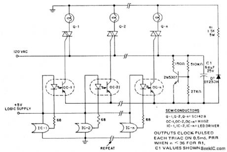
In microprocessor control of multiple loads, the minimum cost per load is critical. A typical application example is a large display involving driving arrays of incandescent lamps. This circuit provides minimal component cost per stage and optocoupler triggering of triac power switches from logic outputs. The minimal component cost is attained by using more complex software in the logic. A darlington output optocoupler provides gate current pulses to the triac, with cost advantages gained from eliminating the current limiting resistor and from the low cost coupler. The trigger current source is a dipped tantalum capacitor, charged from the line via a series resistor with coarse voltage regulation being provided by the darlington signal transistor. The resistor and capacitor are shared by all the darlington-triac pairs and are small in size and cost due to the low duty cycle of pulsing. Coupler IRED current pulses are supplied for the duration of one logic clock pulse (2-10μsec), at 0.4 to 1 msec intervals, front a LED driver LC. The pulse timing is derived from the clock waveform when the logic system requires triac conduction.
A current limiting resistor is not used, which prevents Miller effect slowdown of the H11G2 switching speed to the extent the triac is supplied insufficient current to trigger.Optodarlington power dissipation is controlled by the low duty cycle and the capacitor supply characteristics. (View)
View full Circuit Diagram | Comments | Reading(1566)
50_30000_Hz_WlEN_BRIDGE
Published:2009/7/5 22:23:00 Author:May

Wide-range audio oscillator utilizes high input impedance, high slew rate, and high voltage characteristics of CA3140 opamp in combination with CA3019 diode away. RI and R2 are same value, chosen for frequency desired as given in table.- Circuit Ideas for RCA Linear ICs, RCA Solid State Division, Somerville, NJ, 1977, p 4. (View)
View full Circuit Diagram | Comments | Reading(1295)
STABLE_OPTOCOUPLER
Published:2009/7/5 22:21:00 Author:May

A circuit stabilizes the current-transfer ratio (CTR) of an optically coupled isolator used as a linear transducer. The optocoupler produces a voltage output that is proportional to-but electrically isolated from-the voltage input. However, the output voltage is directly affected by changes in the CTR, and the CTR can change substantially with temperature and current. To a lesser extent the CTR changes with time over the life of the optocoupler. The circuit employs a feedback circuit containing a second optocoupler.
The feedback signal tends to oppose changes in the overall CTR. (View)
View full Circuit Diagram | Comments | Reading(2908)
| Pages:272/471 At 20261262263264265266267268269270271272273274275276277278279280Under 20 |
Circuit Categories
power supply circuit
Amplifier Circuit
Basic Circuit
LED and Light Circuit
Sensor Circuit
Signal Processing
Electrical Equipment Circuit
Control Circuit
Remote Control Circuit
A/D-D/A Converter Circuit
Audio Circuit
Measuring and Test Circuit
Communication Circuit
Computer-Related Circuit
555 Circuit
Automotive Circuit
Repairing Circuit