
Basic Circuit
Index 265
12_V_SHUNT_AT_5_mA
Published:2009/7/6 2:22:00 Author:May
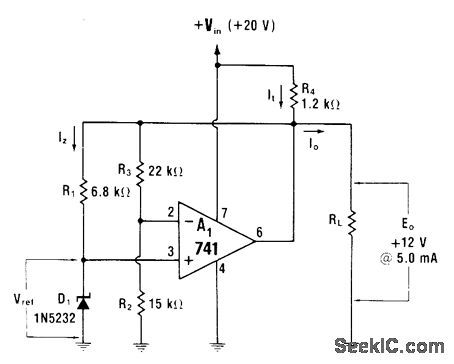
Low-power shunt regulator uses opamp to absorb excess load current. Value of R1 is chosen to step up reference voltage of 5.6-V zener to +12V at 5 mA. Design procedure for other output voltages is given. Output impedance is 0.01 ohm at 100 Hz, giving 120-Hz ripple-frequency filtering comparable to that of 100,000-μF capacitor-W.G. Jung, IC Op-Amp Cookbook, Howard W.Sams, Indianapolis, IN, 1974, p 166-168. (View)
View full Circuit Diagram | Comments | Reading(774)
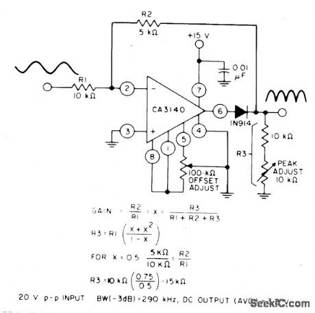
ABSOLUTE_VALUE_IDEAL_FULL_WAVE_RECTIFIER
Published:2009/7/6 2:22:00 Author:May
Circuit Notes
The circuit uses a CA3140 BiMOS op amp in an inverting gain configuration. When equality of two equations shown in satisfied, full-wave output of ctrcuit is symmetril. (View)
View full Circuit Diagram | Comments | Reading(737)
5_V_FROM_48_V
Published:2009/7/6 2:21:00 Author:May

Combillation of zener and resistor R gives equivalent of power zener as solution to regulator protection problem when input voltage is much higher than rated maximum of regulator. Maximum load is 1A. With optional capacitor,circuit noise is only 700μV P-P.-″Linear Applications、Vol.2、″ National Semiconductor,Santa Clara,CA、1976、AN-103,p 10. (View)
View full Circuit Diagram | Comments | Reading(627)
255_FREQUENCY_SYNTHESIZER
Published:2009/7/6 2:21:00 Author:May

Circuit as shown for programmable counter section of Exar XR-2240 programmable timer/counter provides square-wave outputs at 255 discrete frequencies from given internal time-base setting.Output is positive pulse train with pulse width T determined by values of R and C. Period is equal to (N + 1)T where N is programmed count in counter of IC. Counter output connections to output bus determine value of N; if pins 1,3,and 4 are connected to bus, N is 1 + 4 + 8 or 13 and period is 14T, Supply voltage range is 4-.15 V.If counter cannot be triggered when using supplyabove 7V and less than 0.1μF forC, connect 300 pF from pin 14 to ground.- Timer Data Book, Exar Integrated Systems, Sunnyvale, CA, 1978, p 11-18. (View)
View full Circuit Diagram | Comments | Reading(739)
LIGHTS_ON_REMINDER
Published:2009/7/6 2:19:00 Author:May
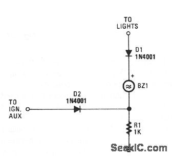
With both the ignition and the car lights on, piezo transducer BZ1 draws no current and remains silent. With only the ignition on, diode D1 is reverse-biased and so prevents current ftow through BZ1.
However, when the lights are on and the ignition is off, the transducer becomes energized and sounds to alert you to turn the lights off. With the ignition off and the lights on, D2 is reverse-biased, preventing current from flowing to the ignition.Resistor R1 prevents a short circuit when the ignitionison is on. (View)
View full Circuit Diagram | Comments | Reading(1089)
UPDATE_TO_100_MHz
Published:2009/7/6 2:16:00 Author:May
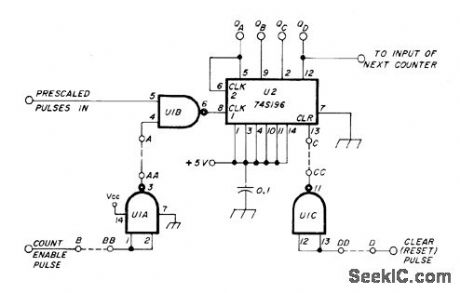
Simple counter stage can be added to input of existing frequency counter to extend direct counting range to 100 MHz, preparing it for use with 1-GHz prescaler.Use 74S196 presettable decade counter and 74S00 NAND-gate IC. If existing counter has positive reset pulse, connect C to CC and D to DD; if reset pulse is negative, connect C to D. If count enable pulse is negative, connect A to AA and B to BB; if positive, connect A to B. Power supply bypass capacitor should be shunted by 47-μF 10-V tantalum or electrolytic. Article covers modifications required in some counter input stages.-I. MacFarlane, How to Modify Your Frequency Counter for Direct Counting to 100 MHz, Ham Radio, Feb. 1978, p 26-29. (View)
View full Circuit Diagram | Comments | Reading(1931)
Microprocessor_supervisory_circuit_with_on_board_chip_enable
Published:2009/7/23 21:37:00 Author:Jessie
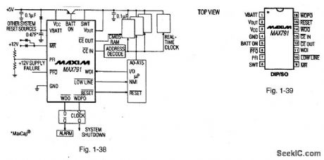
Figures 1-38 and 1-39 show a typical application circuit and pin configuration, respectively, for the MAX791. The IC is similar to that described for Figs. 1-J through 1-M, but with on-board chip-enable. The IC has a 200-ms reset pulse width, 1-μA standby current, 250-mA output in VCC mode, 25-mA output in battery-backup, 1.25-V threshold detector for power-fail warning, low-battery detection, or for monitoring a supply other than +5 V, a separate low-line comparator that compares VCC to a threshold 150 mV above the reset threshold, and a pulsed watchdog output to give advance warning of impending WDO assertion caused by watchdog timeout. MAX[M HIGH-RELIABILITY DATA Book, 1993, P. 5-35. (View)
View full Circuit Diagram | Comments | Reading(661)
12_bit_straight_binary_D_A_converter
Published:2009/7/23 21:37:00 Author:Jessie
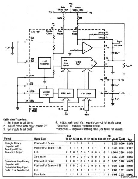
This circuit uses a DAC-4881 and a few external components to form a stand-alone, 0-to -10-V, D/A converter with both gain and offset adjustments for calibration. (View)
View full Circuit Diagram | Comments | Reading(444)
Low_cost_supervisory_circuit_with__3_V_monitoring
Published:2009/7/23 21:37:00 Author:Jessie
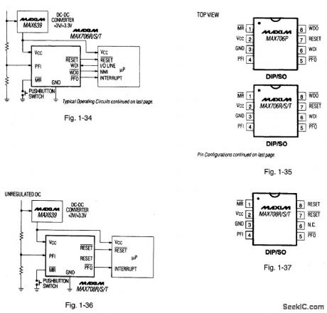
Figures 1-34 and 1-35 show a typical application circuit and pin configurations, respectively, for the MAX706P/R/S/T. Figures 1-36 and 1-37 show a typical application, circuit and pin configuration; respectively, for the MAX708R/S/T The ICs are similar to that described for Figs. 1-J through 1-M, but with the capability of monitoring +3-V supply levels. The ICs have a 200-ms reset pulse width, 100-pA quiescent current, a watchdog with 1.6-s timeout, and a 1.25-V threshold detector for power-fail warning, low-battery detection, or for monitoring supply levels in the +3-V to +5;V range. The difference among the MAX706R,S, and T is the reset-threshold levels, which are 2.63 V, 2.93 V and 3.08 V, respectively. All have active-low reset output signals. The MAX706P reset output is active-high with a 2.63-V threshold. The MAX708R/S/T are identical to the corresponding MAX706, except that the MAX708 series does not have a watchdog, but provides both RESET and RESET outputs. The watchdog is activated when the WDI input has not been toggled within 1,6 s. All of the ICs have an active-low manual reset.MAXIM HIGH-RELIABILITY DATA Book, 1993, P. 5-33, 5-34. (View)
View full Circuit Diagram | Comments | Reading(554)
Typical_testing_troubleshooting_application_of_probe_and_pulser
Published:2009/7/23 21:16:00 Author:Jessie
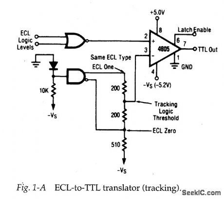
A circuit (such as Fig. 1-A) can be tested by applying a pulse at the input and monitoring the output. This can be done with a pulser (or signal generator) at the in-put and a probe (or scope) at the output. For example, pulses with ECL levels can be applied at the ECL-gate input and TTL pulses can be monitored at the output.If TTL pulses are absent at pin 7 of the 4805 comparator, check for pulses at pins 2 and 3. This procedure will isolate the problem to the gate or to the comparator. (View)
View full Circuit Diagram | Comments | Reading(490)
Low_cost_supervisory_circuit_high_reliability_manual_reset
Published:2009/7/23 21:35:00 Author:Jessie
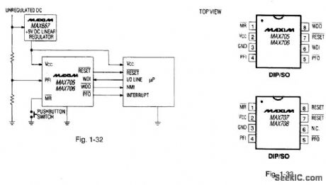
Figures 1-32 and 1-33 show a typical application circuit and pin configurations, respectively, for the MAX705-708. The ICs are similar to that described for Figs. t-J through 1-M, but with generally lower cost. The ICs have a 200-ms reset pulse width, 200-p, A quiescent current, and a 1.25-V threshold detector for power-fail warning, low-battery detection, or for monitoring a power supply other than +5 V.The MAX705/MAX707 generate a reset pulse when the supply is below 4.65V. The MAX706/708 generate a reset below 4.4V. The MAX707/708 is the same as the MAX705/706, except an active-high reset is substituted for the watchdog timer.The watchdog is activated when the WDI input has not been toggled within 1.6 s. MAXIM HIGH-RELIABILITY DATA Book, 1993, P. 5-31. (View)
View full Circuit Diagram | Comments | Reading(743)
General_digital_IC_troubleshooting_tips
Published:2009/7/23 21:21:00 Author:Jessie


The following troubleshooting tips apply to digital circuits where the majority of components are contained in ICs.
Power and ground connectionsThe first step in tracing problems in a digital circuit with ICs is to check all power and ground connections to the ICs. Many ICs have more than one power and one ground connection. For example, the LTC1043 in Fig. 1-B requires +5 V at pins 4 and 5, and -5 V at pin 17. Also, the LTC1090 in Fig. 1-C has both a digital ground (DGND) and an analog ground (AGND). Likewise, the DAC-8565 in Fig. 1-D has both an analog common (pin 5) and a digital common (pin 12).
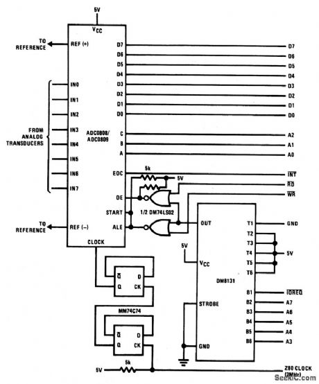
With all power and ground connections confirmed, check that all the ICs receive reset, chip-select, start, and any other function signals, as required. For example, the DAC-4881 in Fig. 1-E requires a chip-select signal at pin 1, as well as address-decode signals at pins 2 and 28. Likewise, the ADC0808/080 in Fig. 1-F requires start, ALE, EOC, and output-enable signals from the microprocessor or control logic. If any of these signals are absent or abnormal (incorrect amplitude, improper timing, etc.) circuit operation comes to an immediate halt.In some cases, control signals to digital ICs are pulses (usually timed in a certain sequence) and other control signals are steady (high or low). If any of the lines carrying the signals to the ICs are open, shorted to ground, or to power (typically +5 V or +12 V, and 3 V or 3.3 V for newer digital circuits), the IC will not function. So, if you find an IC control pin that is always high, always low, or apparently is connected to nothing (floating), check the PC traces or other wiring to that pin carefully.As an example, when the DAC4881 is connected as a 12-bit straight-binary digital-to-analog converter (Chapter 6) as shown in Fig. 1-G, the chip-select (pin 1) and address-decode (pins 2, 28) are connected to ground. If the DAC4881 is connected as an 8-bit with complementary input DAC (Fig. 1-E), the chip-select must receive a write (WR) signal, and the address-decode pins must receive address bits from the microprocessor.
(View)
View full Circuit Diagram | Comments | Reading(946)
DUAL_CONVERSION_SYNTHESIZER
Published:2009/7/6 2:15:00 Author:May
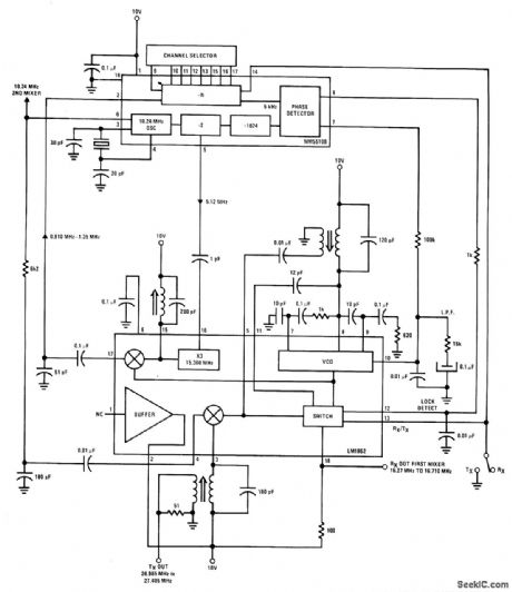
Singlecrystal transceiver system uses 10.240-MHz reference frequency which is added to VC0 frequency to produce transmit frequency. Same 10.240-MHz reference frequency is mixed with first IF signal to generate 455-kHz second IF signal. Dividing reference by 2 provides 5.120-MHz signal that is lightly coupled to multiply-by-3 buffer whose output is tuned to third harmonic (15.360 MHz). This is mixed with VCO frequency to provide input signal for programmable divider, When VCO is operating as first mixer and local oscillator on CB channel 1 (16.270 MHz), difference frequency is 910 kHz. Programmable divider divides by 182 to give necessary 5-kHz input to phase detector. If VCO moves off frequency, divided input to phase detector moves away from 5 kHz and action of loop pulls VC0 back on frequency.-L. Sample, A Linear CB Synthesizer, IEEE Transactions on Consumer Electronics, Aug. 1977, p 200-206. (View)
View full Circuit Diagram | Comments | Reading(676)
10_1_PRESCALER_FOR_500_MHz
Published:2009/7/6 2:14:00 Author:May
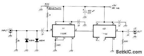
Uses Fairchild 11C06 D flip-flop and Fairchild 95H91 divide-bp 5 counter. Input sensitivity is less than 100 mV from 10 to 500 MHz. Back-to-back diodes protect 11C06 input from overloads. Output is fed to 50-MHz frequency counter. Use regulated supply.-W, C. Ryder, 500-MHz Decade Prescaler, Ham Radio, June 1975, p 32-33. (View)
View full Circuit Diagram | Comments | Reading(2107)
Z80_interface_with_partial_decoding_for_A_D_converter
Published:2009/7/23 21:20:00 Author:Jessie
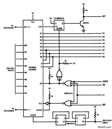
This circuit shows a Z80 interface for the ADC0808/0809 where the DM8131 decodes 5 address bits and the IOREQ I/O request strobe. Two NOR gates gate the RD and WR strobes for ALE, START, and OE inputs. (View)
View full Circuit Diagram | Comments | Reading(1058)
Basic_positive_reference__DAC
Published:2009/7/23 21:27:00 Author:Jessie
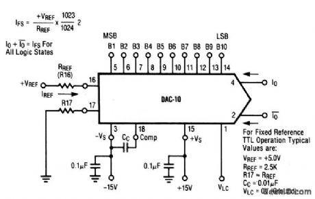
This circuit shows a DAC that is connected for positive-reference D/A-converter operation.
(View)
View full Circuit Diagram | Comments | Reading(469)
Microprocessor_supervisory_circuit
Published:2009/7/23 21:27:00 Author:Jessie
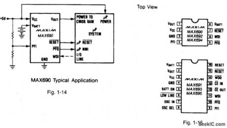
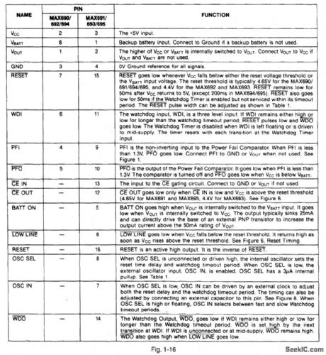
Figures 1-14 and 1-15 show a typical application circuit and block diagram, respectively, for the MAX690. The IC is similar to that described for Fig. 1-M, but also includes watchdog and battery-backup protection, and has a 1.3-V threshold detector, as shown in Fig. 1-16. Use the equations shown in Fig. 1-M to calculate the values for the resistors at the PFI input (except use a threshold of 1.3 V, instead of 2.54 V). MAXIM NEW RELEASES DATA Book, 1992, P. 5-19, 5-22. (View)
View full Circuit Diagram | Comments | Reading(1221)
LOW_HYSTERESIS_TRIGGER
Published:2009/7/23 21:26:00 Author:Jessie
Differential-amplifier pair, with constant-current source Q3 replacing emitter resistor, serves as level detector with low hysteresis. Good up to 60 kc.-D. B. Campbell, Low-Hysteresis Trigger Circuits, EEE, 13:1, p 76. (View)
View full Circuit Diagram | Comments | Reading(771)
AUTOMOBILE_IGNITION_SUBSTITUTE
Published:2009/7/6 2:14:00 Author:May
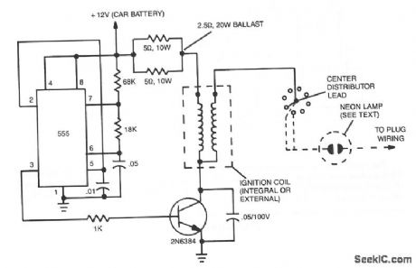
The ignition substitute provides a constant power source for the ignition coil. Its frequency, 0.5- 1.0 kHz, is that used by an 8-cylinder engine with an idling speed of 650 RPM, and the unit provides a rapid spark at a 17% duty cycle, while staying within the power dissipation limits of the components.
The circuit consists of a 555 timer IC configured as an astable free-running multivibrator that is used to drive a high-current npn transistor, such as a 2N6384. The transistor should be heavily heatsinked because it might be drawing several amps over quite a long period of time.
The coil ballast can be from 0.68 to 6.5Ω, depending on what's available. The 2.5-Ω, 20-W ballast shown works well. All the other resistors can be either 1/4- or 1/2-W devices, and the capacitor, between pins 1 and 5 of the 555, can range from 0.01 to 0.05 μF. Do not omit the 100-V, 0.05-μF capacitor across the transistor; it prevents voltage spikes from damaging the device.
Although designed for an 8-cylinder engine, this device can be used with other types. In addition,a neon bulb can be added to the circuit to verify the presence of a spark.
(View)
View full Circuit Diagram | Comments | Reading(727)
Microprocessor_monitor
Published:2009/7/23 21:25:00 Author:Jessie
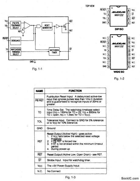
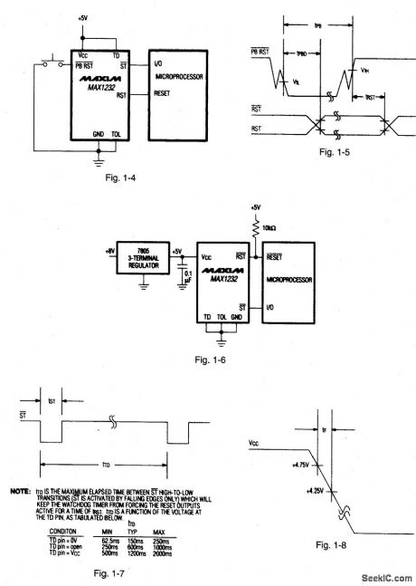
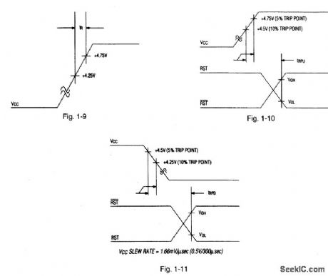
Figures 1-1, 1-2, and 1-3 show the block diagram, pin configuration and pin description, respectively, for the MAX1232. The IC is similar to that described for Figs. 1-K and 1-L, except that only '/to power is consumed. Figures 1-4 and 1-5 show the basic connections and waveforms, respectively, for the pushbutton reset.Figures 1-6 and 1-7 show the basic connections and waveforms, respectively, for watchdog timing. Notice that the software routine that strobes ST is critical. The code must be in a section of software that executes frequently enough so that the time between toggles is less than the watchdog timeout period, as shown in Fig. 1-7. Figures 1-8 and 1-9 show the power-down and power-up slew rate, respectively.Figures 1-10 and 1-11 show the VCC-detect reset-output delays. MAXIM NEW RELEASES DATA BOOK, 1992, P. 5-11, 5-14, 5-:5, 5-16. (View)
View full Circuit Diagram | Comments | Reading(673)
| Pages:265/471 At 20261262263264265266267268269270271272273274275276277278279280Under 20 |
Circuit Categories
power supply circuit
Amplifier Circuit
Basic Circuit
LED and Light Circuit
Sensor Circuit
Signal Processing
Electrical Equipment Circuit
Control Circuit
Remote Control Circuit
A/D-D/A Converter Circuit
Audio Circuit
Measuring and Test Circuit
Communication Circuit
Computer-Related Circuit
555 Circuit
Automotive Circuit
Repairing Circuit