
Basic Circuit
Index 269
100_kHz_WIEN_BRIDGE
Published:2009/7/6 0:46:00 Author:May

CA3160 opamp in bridge circuit oporates from single 15-V supply. Paralle-connected diodes form gain-setting network that stabilizes output voltage at about 1.1 V. 500-ohm pot is adjusted so oscillator always starts and oscillation is maintained.- Linear Integrated Circuits and MOS/FET's, RCA Solid State Division, Somerville, NJ, 1977, p 271-272. (View)
View full Circuit Diagram | Comments | Reading(1679)
CRYSTAL_SWITCHING_DIODES
Published:2009/7/6 0:44:00 Author:May

Circuit for Motorola MC12060 crystal oscillator uses diodes as BF switches giving choice of five different crystal frequencies Forward bias is applied to diode associated with desired crystal and reverse bias to diodes for other four crystals. Diode switching eliminates need to run high-frequency signals through mechanical switch, permits control of switching from remote location, and is readily adapted to electronic scanning. Requires only single 5-V supply. Frequency pulling is minimized.-J. Hatchett and R. Janikowski, “Crystal Swtiching Methods for MC12060/MC12062 Oscillator,” Motorola, Phoenix, AZ, 1975, AN-756. (View)
View full Circuit Diagram | Comments | Reading(697)
DAC_current_loop_controller
Published:2009/7/25 5:40:00 Author:Jessie

Figure 9-41 shows a DAC0830 connected to provide digital control ofthe standard 3-mA to 20 mA industrial-process current loop. The circuit is two-terminal, and all circuit components (including the DAC) are powered directly from the loop,The output transistor conducts whatever current is necessary to keep the voltage across R3 equal to the voltage across R2.This voltage and therefore the total loop current is directly proportional to the output current from the DAC. The net resistance of R1 is used to set the zero-code loop current to 4 mA and R2 is adjusted to provide the 16-mA output span for a full-scale DAC code. The entire circuit floats by operating whatever ground-reference potential is required for the total loop resistance andloop current,The voltage differential between the input and output terminals mustbe kept in the range of 16 V to 55 V and the digital inputs to the DAC must beelectronically isolated from the ground potential. of the controlling microprocessor.This isolation can best be achieved with opto-isolators.in a non microprocessor system in which the loop-controlling information comes from thumb wheel switches(or a similar mechanical device) the digital input for the DAC can be taken from BCD-to-binary CMOS logic elements (which are ground referenced to the groundpotential of the DAC).The total Supply current requirements of all circuits usedmust (of course) be less than 4 mA and R1 can be adjusted accordingly. NATIONAL SEMICONDUCTOR, APPLICATION NOTE 271. 1994. P. 670. (View)
View full Circuit Diagram | Comments | Reading(754)
DAC_high_current_controller
Published:2009/7/25 5:38:00 Author:Jessie
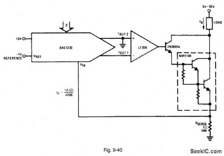
Figure 9-40 shows a DAC1230 connected to provide digital control of a 1-A current sink. Such a circgit can be used for heater control, stepper-motor torque compensation, and automatic test equipment. The largest source of nonlinearity in this circuit is the stability of the current-sensing resistance (with changes in power dissipation). The sensing resistance should be kept as low as possible to minimize this effect. The reference voltage must be reduced (to -1 V, as shown) to maintain the output-current range. The triple Darlington is used to minimize the base-current flowing through the sensing resistance, while simultaneously maintaining the collector current flow to the load. NATIONAL SEMICONDUCTOR, APPLICATION NOTE 271, 1994, P. 669. (View)
View full Circuit Diagram | Comments | Reading(757)
65_110_MHz_OVERTONE
Published:2009/7/6 0:42:00 Author:May
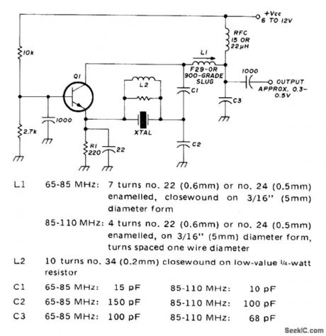
Uses fifth- or seventh-overtone crystals. RF choke formed by L2 is wound on low-value resistor to suppress lower-frequency resonances of crystal. Buffer is recommended. Circuit is slightly frequency-sensitive to supply voltage variations, so use well-regulated supply. Q1 is 2N3563, 2N3564, 2N5770, BF180, BF200, or SE1010.-R. Harrison, Survey of Crystal Oscillators, Ham Radio, March 1976, p 10-22. (View)
View full Circuit Diagram | Comments | Reading(864)
1365_Hz_TONE
Published:2009/7/6 0:41:00 Author:May
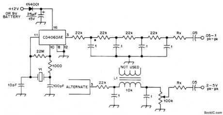
Uses 2.235-MHz crystal with counter chip to produce 136.5-Hz subaudible tone for amateur transmitter. Low-frequency square-wave output of IC is put through multistage low-pass filter to develop sine wave. Tone should be introduced into transmitter just after audio processing (after deviation control). AIternate filter is also shown; use whichever gives best performance, For other tone frequency, use crystal that is 16,384 times frequency desired.-E. Gellender and M. Marcel, P/L Tone Generator, QST, Aug. 1976. p 43. (View)
View full Circuit Diagram | Comments | Reading(553)
CAPACITIVELY_TUNED_WIEN
Published:2009/7/6 0:41:00 Author:May
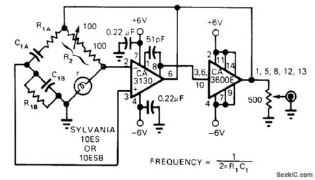
Output of amplifier is connected to apex of Wien bridge. Positive feedback is taken from junction of C1A and C1B for noninverting input of first opamp, while negative feedback is taken from other junction of bridge for inverting input. Oscillation is sustained when R2 = 2r. Nonlinearity of lamp r provides stabilization of oscillator. Frequency depends on values used for bridge components.-H. D. Olson, Wien-Bridge Oscillator Is Capacitively Tuned, EDN Magazine, Aug. 5, 1975, p 74. (View)
View full Circuit Diagram | Comments | Reading(542)
2_22_MHz_FUNDAMENTAL_MODE
Published:2009/7/6 0:37:00 Author:May
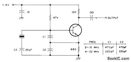
International Crystal OF-1 oscillator for fundamental-mode crystal has no LC tuned circuits and lei quires no inductors. With 28.3-MHz third-overtone crystal, output is at fundamental of crystal or about 9.43 MHz,-C. Hall, Overtone Crystal Oscillators Without Inductors, Ham Radio, April 1978, p 50-51. (View)
View full Circuit Diagram | Comments | Reading(1057)
OSCILLATOR_DOUBLER
Published:2009/7/6 0:36:00 Author:May
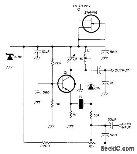
Overtone crystal oscillator circuit that frequency-doubles in transistor can be frequency-modulated or used as stable voltage-controlled crystal oscillator. Tuning range with 70-MHz third-overtone crystal is typically 30 kHz at crystal frequency or 60 kHz at output. L1 is resonant with C1 at desired out-put frequency. Tap for varactor CR1 (Motorola BB 105B or BB142) is at one-fourth total number of turns. Q1 is 2N918, BF115, HEP709, or equivalent.-U. Rohde, Stable Crystal Oscillators, Ham Radio, June 1975, p 34-37. (View)
View full Circuit Diagram | Comments | Reading(2006)
WlEN_BRIDGE_2_W
Published:2009/7/5 23:57:00 Author:May
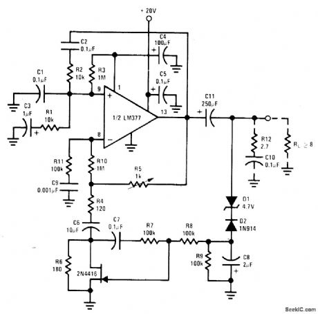
Uses haff of LM377 IC connected as oscillator, with FET amplitude stabiIization in negative feedback path. Total harmonic distortion is under 1% up to 10 kHz. With values shown, maximum output is 5.3 VRMS at 60 Hz. R12 and C10 are added if necessary to prevent high-frequency instability.- Audio Handbook, National Semiconductor. Santa Clara. CA. 1977. p 4.8-4-20. (View)
View full Circuit Diagram | Comments | Reading(592)
Reset Timing Circuit of Power Supply Connection
Published:2011/7/25 23:39:00 Author:Michel | Keyword: Power Supply, Reset Timing Circuit

Picture 1 is reset circuit of power supply connection.The function of NE555 feet 4 is that it works when it is connected to high PWL and it resets when it is connected to low PWL.R3 and C2 are connected to feet 4,this circuit has time constant functions. Therefore, the power supply is connected,feet 4 won't rise to + Ucc immediately,which needs R3 and C2 constant delay.In this period, even if feet 2 inputs pulse, feet 3 trigger output still remains low level.R2 and R4 are ME555 current limiting resistance and TTL level triggering pulse triggers NE555 feet 2 directly via R2.VD1 is the diode which makes C2 discharge fast when the power supply is off and it outputs pulse width T=R5C4. (View)
View full Circuit Diagram | Comments | Reading(646)
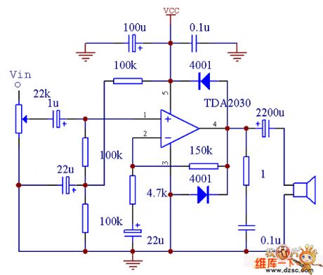
TDA2030 power amplifier circuit double power connecting method circuit diagram
Published:2011/7/13 9:36:00 Author:Nancy | Keyword: power amplifier, double power, connecting method

The power rating of TDA2030 power amplifier circuit double power connecting method is 14W. The power supply voltage is + 6 ~ + 18 V. Output current is big, harmonic distortion and crossover distortion is small (+ 14 V/4 ohms, THD = 0.5%). (View)
View full Circuit Diagram | Comments | Reading(3199)
PANORAMIC_FRONT_END
Published:2009/7/23 21:45:00 Author:Jessie
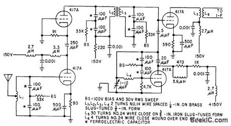
Can be made as three plug-in units, each containing the electrically tunable r-f, mixer, and local oscillator stages to cover 35 to 70, 70 to 130, and 130 to 200 Mc. Each plug-in front end has eight voltage-tunable ferroelectric tuners.-T. W. Butler, Jr., Ferroelectrics Tune Electronic Circuits, Electronics, 32:3, p 52-55. (View)
View full Circuit Diagram | Comments | Reading(426)
TDA2030 power amplifier circuit single power connecting method circuit diagram
Published:2011/7/13 9:37:00 Author:Nancy | Keyword: power amplifier, single power, connecting method,
The power rating of TDA2030 power amplifier circuit double power connecting method is 14W. The power supply voltage is + 6 ~ + 18 V. Output current is big, harmonic distortion and crossover distortion is small (+ 14 V/4 ohms, THD = 0.5%). (View)
View full Circuit Diagram | Comments | Reading(1791)
Binary Synchronous Counter Circuit of 74HC161
Published:2011/7/25 10:24:00 Author:Michel | Keyword: Binary, Counter Circuit

Picture 1 is binary synchronous counter circuit of 74HC161.It needs the counter which issynchronous with clock to get the real time counting result.When the highest clock frequency is input,the gate circuit is used,the front level (74HC161(1))RCO input is added to ENP of the last level (74 HCl61 (4).Therefore, the signal delay is determined by gate and it has nothing to do with counter so that the clock frequency is increased.In the circuit, the CLR, LD, CLK ENB are extra signals.When the CLR is low PWL,Qo一Q15 outputs low PWL.When ENB is high PWL,CLK rising edge is counting.
Picture 1:Binary Synchronous Counter Circuit of 74HC161
(View)
View full Circuit Diagram | Comments | Reading(3748)
BLOWN_FUSE_BLINKER
Published:2009/7/5 23:54:00 Author:May

Neon,lamp NE-2 glows steadily when fuse is good and flashes when fuse opens. Flash rate, determined by R1 and C1, is about to flashes per second for values shown.-T.Lincoln, A Smart Blown-Fuse In.dicator, QST, March 1977, p 48. (View)
View full Circuit Diagram | Comments | Reading(834)
5_V_FET_REGULATOR
Published:2009/7/5 23:52:00 Author:May

Output voltage changes less than 0.1 V for load current change from 0 to 60 mA. Output voltage changes caused by change in load resistance affect gate-source voltage of FET Tr1 via R1 and R2, causing compensating change in drain cument. Additional transistors serve to reduce output resistance and increase output current without affecting stabilization ratio of about 1000.-C. R. Masson, F.EJf. Voltage Regulator, Wireless World, Aug.1971, p 386. (View)
View full Circuit Diagram | Comments | Reading(538)
Basic_flash_memory_VSUBPP_SUB_programming_voltage_supply
Published:2009/7/23 22:02:00 Author:Jessie
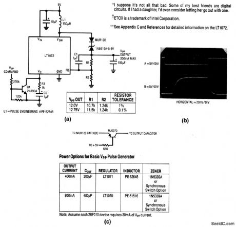
This circuit provides VPP (program power) pulses for programming digital flash memories. Figure 6-48 shows the waveforms involved. Trace A is the programming command. Trace B shows a smoothly rising VPP pulse of the correct amplitude. The amplitude of VPP can be selected by the values of R1 and R2. Figure 6-48C shows a synchronous switch option for the circuit, as well as output currents available with the option. (View)
View full Circuit Diagram | Comments | Reading(701)
_30V_TO__7V
Published:2009/7/5 23:51:00 Author:May
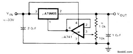
Circuit uses Signetics μA79M05 adjustable voltage regulator in combination with 741 opamp to give wide negative output voltage range. Regulator includes thermal overload protection and internal short-circuit protection. Input voltage should be at least 3V more negative than maximum output volt-age desired.- Signetics Analog Data Manual, Signetics, Sunnyvale, CA, 1977, p 670. (View)
View full Circuit Diagram | Comments | Reading(478)
NON_INTEGER_PROGRAMMABLE_PULSE_DIVIDER
Published:2009/7/5 23:46:00 Author:May
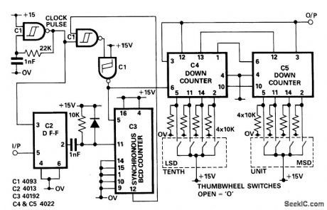
Circuit NotesIn applications where the period of the input pulses is uneven and the divider is required to cover a wide range of frequencies, the non-integer programmable pulse divider shown can be used. The purpose of the D-type flip-flop (IC2) is to synchronize the input signal with the clock pulse. When the clock pulse changes from low to high and the input is high, IC2 output goes high. Subsequently, IC3 resets to zero and starts counting up.The number of pulses at the output of IC3 is ten time the input pulse. IC4 and IC5 are cascaded to form a two decade programmable down counter. (View)
View full Circuit Diagram | Comments | Reading(1010)
| Pages:269/471 At 20261262263264265266267268269270271272273274275276277278279280Under 20 |
Circuit Categories
power supply circuit
Amplifier Circuit
Basic Circuit
LED and Light Circuit
Sensor Circuit
Signal Processing
Electrical Equipment Circuit
Control Circuit
Remote Control Circuit
A/D-D/A Converter Circuit
Audio Circuit
Measuring and Test Circuit
Communication Circuit
Computer-Related Circuit
555 Circuit
Automotive Circuit
Repairing Circuit