
Basic Circuit
Index 263
UHF_PRESCALER
Published:2009/7/6 3:15:00 Author:May

Uses Fairchild 11C06 700-MHz D flip-flop as divide-by-20 UHF prescaler with toggle rates in excess of 550 MHz from 0 to 75°C. Amplifier may be used in place of input bias network shown. Developed for use with 95H9O decade divider. Unused CP and D inputs are tied to ground.-D. Schmieskors, 1200-MHz Frequency Sealers, Ham Radio, Feb. 1975, p 38-40. (View)
View full Circuit Diagram | Comments | Reading(926)
AUTOMOBILE_AIR_CONDITIONER_SMART_CLUTCH
Published:2009/7/6 3:12:00 Author:May

This circuit disables the air conditioner compressor when additional engine power is required. It does so by monitoring the engine vacuum at the intake manifold. If the vacuum drops to 40% of its normal level, the compressor clutch is disabled, removing the air conditioner load from the engine. After the engine returns to normal vacuum level, there is a 6 second delay before the compressor clutch is enabled and the air conditioner is reactivated. This allows 6 seconds of extra power, about 500 ft at 60 MPH, which increases the safety margin when passing another vehicle. Loss of cooling is minimal because the air conditioner fan is not interrupted. When the engine is accelerated, manifold vacuum drops and vacuum switch VS opens to 40% of the normal manifold pressure. This causes Q1 to turn on, discharging C2 and tuming off Q3 via diode D2. When Q3 tums off, so does Q2. When the engine reaches its normal operating vacuum, VS closes and Q1 turns off, allowing C2 to charge for 6 seconds until Q3 turns on again.
(View)
View full Circuit Diagram | Comments | Reading(534)
PLL_DIVIDER
Published:2009/7/6 3:11:00 Author:May

Simple phase-locked loop is suitable for generating integral submultiples M of input frequency. Values shown give M of 2.Square-wave input reference is limited in amplitude to supply voltage by first CMOS inverter A3A. RC network R9-C2, integrates output to give 2 V P-P triangle across C2 for sampling by sample-and-hold switch sections S1 and S2 of 4016 CMOS analog switch. Sampled error voltage of loop, stored on CH2, is read out by FET amplifier A2. Amplified error voltage is applied to A1 through R5 to induce changes in center frequency of A1 as required to maintain locked condition.-W. G. Jung, IC Timer Cookbook, Howard W. Sams, Indianapolis, IN, 1977, p 220-224.
(View)
View full Circuit Diagram | Comments | Reading(969)
_15_V_WITH_FEEDBACK
Published:2009/7/6 3:10:00 Author:May

Fraction of output voltage is fed back to base of 2N3641 regulator transistor. Difference between this voltage and zener diode voltage is amplified to control base of 2N5191 series transistor.-H. Olson, Powet-Supply Servicing, Ham Radio, Nov. 1976, p 44-50. (View)
View full Circuit Diagram | Comments | Reading(1163)
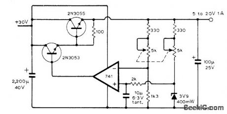
71_65V_AT_0_1_A
Published:2009/7/6 3:09:00 Author:May
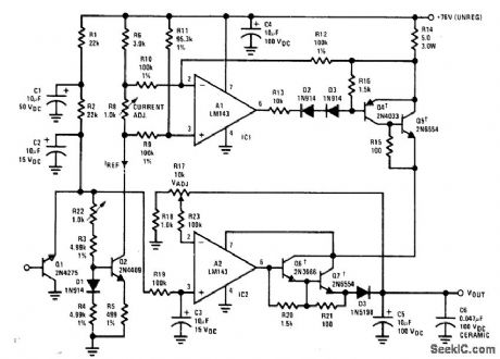
Provides continuously variable output voltage and adjustable output cur-rent range. Q1 is connected as zener to give 6.5-V reference voltage. Darlington current boosters Q4-Q7 should be on common Thermafloy 60068 or equivalent heatsink. Developed for use with pulsed loads. For input volt-age range of 46-76 V, regulation is within 286 mV for 500-mA DC output.- Linear Applica-tions, Vol. 2, National Semiconductor, Santa Clara, CA, 1976, AN-127, p 8-10. (View)
View full Circuit Diagram | Comments | Reading(636)
_15_V_FROM_HIGH_INPUT_VOLTAGE
Published:2009/7/6 3:08:00 Author:May
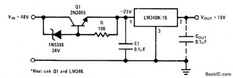
Zener is used in series with resistor R to level-shift input voltage higher than rated maximum of LM340K-15 regulator. Typical load regulation is 40 mV for 0-1 A pulsed load, and line regulation is 2 mV for 1-V change in input voltage for no load.With optional output capacitor, circuit noise is only 700 ptV P-P.- Linear Applications, Vol. 2, National Semiconductor, Santa Clara, CA, 1976, AN-103,p9-10. (View)
View full Circuit Diagram | Comments | Reading(1645)
6800_interface_with_partial_address_decoding_for_A_D_converter
Published:2009/7/23 21:02:00 Author:Jessie
This circuit shows a typical6800 interrupt interface for the ADC0808/ 0809 using a flip-flop and an open-collector transistor. The interrupt is reset when the data bits are read. Figure 6-25B shows routine. (View)
View full Circuit Diagram | Comments | Reading(1225)
DUAL_TIMER_TONE_STEPPER
Published:2009/7/6 3:08:00 Author:May

One section of RS556 dual timer is connected as free-running astable MVBR for supplying pulses to trigger input of other section connected as mono MVBR driving loudspeaker. When both MVBRs are adjusted so one trigger pulse initiates each timing period and no trigger pulses occur during timing pefiods, output tone has frequency of freerunning MVBR. With two trigger pulses per timing cycle, every other trigger pulse is ignored and tone is at half frequency. With three trigger pulses per cycle, output is one-third of frequency. Can be used for classloom demonstration of electronic music;settings of R1 and R3 can be adjusted to give tones regembling violin, bagpipes, or almost any other instrument.-F. M. Mims, Integrated Circuit Projects, Vol. 6, Radio Shack, Fort Worth, TX, 1977, p 70-78. (View)
View full Circuit Diagram | Comments | Reading(587)
100_mA_CURRENT_REGULATOR
Published:2009/7/6 3:07:00 Author:May
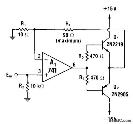
741 opamp is connected as noninverting voltage-controlled cuwent source feeding transistors that boost output and provide bidirectional current capability in load RL.If single-polarity currentflow is sufficient, omit opposite-polarity transistor.-W. G. Jung, IC Op-Amp Cookbook, Howard W. Sams, Indianapolis, IN, 1974, p 173. (View)
View full Circuit Diagram | Comments | Reading(4995)
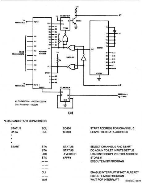
8080_8224_8228_interrupt_type_interface_for_A_D_converter
Published:2009/7/23 20:56:00 Author:Jessie

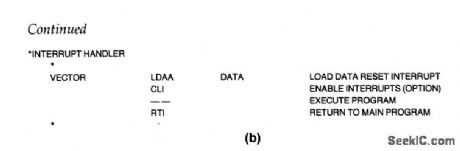
This circuit shows an interrupt-type interface for the ADC0808/0809 using a 6-bit bus comparator to decode a read-and-write strobe. Viewed from the CPU, this interface looks like a bidirectional data port where the address is set by the logic levels on the in inputs of the DM8131. When data bits are written to the ADC, the 3 least-significant bits on the address bus define the channel to be converted. The rest of the bits are decoded to provide the START and ALE strobes (Fig. 6-13B). When the conversion is completed, EOC sets the interrupt flip-flop, and (when the data bits are read) the interrupt is complete. (View)
View full Circuit Diagram | Comments | Reading(1699)
DIVIDER_WITH_PULSE_SHAPER
Published:2009/7/6 3:07:00 Author:May

Hah of Exar XR-2556 dual timer divides input pulse frequency by 2 or 3, and other haff shapes output pulse by controlling duty cycle over range that can be adjusted from 1% to 99% with R,. Supply voltage can be 4.5-16 V.- Timer Data Book, Exar Integrated Systems, Sunnyvale, CA, 1978, p 23-30. (View)
View full Circuit Diagram | Comments | Reading(667)
5_20_V_ZENER_STABILIZED
Published:2009/7/6 3:06:00 Author:May
Use of dual linear pot simplifies problem of feeding reference zener diode from variable-voltage supply.-L.J Baughan, Vatiable Power Supply with Zener Stabilization, Wireless World, Nov. 1975、p 520 (View)
View full Circuit Diagram | Comments | Reading(687)
DIVIDER_FOR_7_MHz
Published:2009/7/6 3:05:00 Author:May
Used after 7-MHz VFO of 40-meter transmitter, to provide 3.5 MHz as required for operation in 80-meter band. Half of 7474 TTL D flip-flop Un is connected in divide-by-2 configuration. U2 provides required well-regulated 5-V source. Q1 clips negative-going portion of 7-MHz sine wave to prevent damage to 7474. Square-wave 3.5-MHz output from U1 is applied to source-follower Q2 which drives class A amplifier output stage Q3. RFC1 and RFC2 are 10 μH. C1 is 6.8-μF 10-V tantalum. Q2 is 100-pF mica. L1 is 41 turns No. 26 enamel spaced to fill entire 7-80-2 core,to give 10 ptH.-S. Creason, A VFO Frequency Divider, QST, Nov. 1976, p 23-24.
(View)
View full Circuit Diagram | Comments | Reading(2196)
8080_8224_8228_Polled_interface_for_A_D_converter
Published:2009/7/23 20:54:00 Author:Jessie


This circuit shows a polled interface for the ADC0808/0809.where the address is partially decoded by a DM74LS139, which creates the read and write strobes to operate the ADC. The circuit can be connected in an interrupt mode using resettable latches (as shown in the dashed lines of Fig. 6-20). Figure 6-23B shows typical polled routines. (View)
View full Circuit Diagram | Comments | Reading(575)
AF_DlVlSlON_BY_2_TO_11
Published:2009/7/6 3:03:00 Author:May
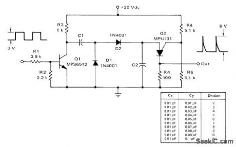
Ratio of C2 to C1 determines division ratio, as given in table. When C2 charges to peak point firing voltage of Q2, it fires and discharges C2, so C1 charges to line voltage. Q2 then turns off. Next cycle begins with another positive pulse on base of Q1, discharging C1. Division range can be chanced by utilizing programmable aspect of PUT Q2 and changing ratio of resistances.-R. J. Haver and B. C. Shiner, Theory, Characteristics and Applications of the Programmable Unijunetion Transistor, Motorola, Phoenix, AZ, 1974 AN-S27, p 9. (View)
View full Circuit Diagram | Comments | Reading(684)
DIVIDING_40_60_MHz_BY_2_3_OR_4
Published:2009/7/6 3:01:00 Author:May

Division ratio is controlled externally by making control terminals A and B high (1) or low (0), as given in table. Developed for use in receiver requiring local oscillator covering 10 to 30 MHz. Counter simplifies tuner design.-C. Attenborough, Fast Modulo-3 Counter, Wireless World, Aug. 1976,p 52. (View)
View full Circuit Diagram | Comments | Reading(855)
WIDE_BANDWIDTH_PEAK_DETECTOR
Published:2009/7/6 3:00:00 Author:May

This circuit can detect the positive peaks for signal frequencies higher than 5 MHz. It yields ±1% accuracy for 400 mV to 4 V pk-pk signal amplitudes on sine, square, and triangular waveforms. The Am685 comparator output increases whenever VIN is a greater negative voltage than VOUT; the high comparator output, in turn, charges C1 in a positive direction. The CA3140 op amp amplifies the C1 voltage with respect to the ECL-switching-threshold voltage (- 1.3 V) developed by diodes D1 and D2. For repetitive waveforms, each cycle boosts VOUT until it equals the peak input value. The peak-detection process is aided by the comparator's open-emitter output, which allows C1 to charge rapidly through R2, but to discharge slowly through R2 and R1. Reducing the value of C1 shortens system-response times. Although the circuit can't detect negative-going peaks, it can be modified to measure the pk-pk value of bipolar signals that are symmetric about ground. To do so, divide VOUT by 2 using two 1-KΩ resistors and feed the comparator VOUT/2 rather than VOUT. (View)
View full Circuit Diagram | Comments | Reading(1118)
DIVIDE_BY_9_WITH_SHIFT_REGISTER
Published:2009/7/6 2:59:00 Author:May

Uses 7496 as 5-bit shift register,7486 as EXCLUSIVE-OR gate,and 7404 as inverter to give division of square-, aveinput frequency by 9 while main-taining 50% duty cycle at output Article covorsconnection changes needed for other divisionratios,With 8-bit shiftregister,circuit, divideby as much as 15,Addition of,486 EXCLUSIVE-OR gate across any outputs,as shown by dashed lines,makes effective output har that of basic TTL circuit,-J,N,Hobbs,Jr.,Divide-by-N Uses Shift Register,EDN Magazine,Oct 5,1976,p 108.
(View)
View full Circuit Diagram | Comments | Reading(2223)
DIVIDE_BY_7
Published:2009/7/6 2:58:00 Author:May

Requires only two differenttypes of chips. Input clock is alternately inverted and noninverted by gates operating in conjunction with 3 bits of storage using 852, to give squarewave output at one-seventh of clock frequency.-C. W. Hardy, Reader Responds to Odd Modulo Divider in July 1st EDN, EDN Magazine, Oct. 1, 1972, p 50. (View)
View full Circuit Diagram | Comments | Reading(683)
001_Hz_TO_100_kHz
Published:2009/7/6 2:53:00 Author:May
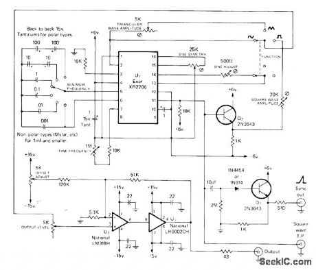
Variable DC offset permits adjustment of average value of sine, square, or triangle waveform to any arbitrary plus or minus value within voltage swing capability of opamp U3 Buffer stage U2 is inside feedback loop. Simple emitter-follower differentiator provides positive-going 1-V 0.5-μs output at sink terminal. Square-wave output is buffered by emitter-follower Q2.-H.Olson, The Function Generator, CQ, July 1975, p 26-28 and 71-72. (View)
View full Circuit Diagram | Comments | Reading(1014)
| Pages:263/471 At 20261262263264265266267268269270271272273274275276277278279280Under 20 |
Circuit Categories
power supply circuit
Amplifier Circuit
Basic Circuit
LED and Light Circuit
Sensor Circuit
Signal Processing
Electrical Equipment Circuit
Control Circuit
Remote Control Circuit
A/D-D/A Converter Circuit
Audio Circuit
Measuring and Test Circuit
Communication Circuit
Computer-Related Circuit
555 Circuit
Automotive Circuit
Repairing Circuit