
Basic Circuit
Index 277
MULTIPLES_OF_25_MHz
Published:2009/7/4 21:19:00 Author:May
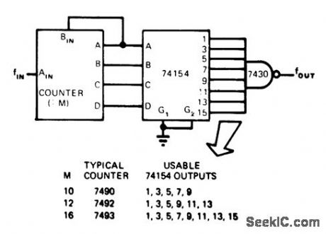
Three TTL circuits provide integral frequency-multiplication ratiosbetween1 and 8. BCD outputs of counter having modulus M are fed to inputs of 74154 4-line to16-line decoder.As outputs of counter change、at rate equal to input frequency divided by counter modulus M,each goes low at samerate Output of NAND gatethus goes high oncefor each input to gate from decoder.If 7490 decade counter is used and inputis 1 MHz,BCD outputs of 7490limit usable outputs of 74154 to lines 1,3,5,7,and 9.Since inputs to 74154 change at l00-kHz rate,output from gate will be n×100 kHz .With inρut of 25 MHz、output is integral multiple of 2.5MHz.-R .s Stein,Three TTLIC's Provide Frequency Multiplication,EON Magazine,April 5、1975、p 117 and 119. (View)
View full Circuit Diagram | Comments | Reading(1493)
SQUARER
Published:2009/7/4 21:04:00 Author:May

Simple tunnel-diode circuit doubles frequency efficiently without use of tuned circuits. Fundamental and other harmonics of input areat least 30 dB below level of frequencydoubled output. Circuit operates from DC to upper frequency limit of opamp used. Adjust R2 so diode current is at peak of its bias current, to eliminate offset at amplifier output.-R. Kincaid, Squaring Circuit Makes Efficient Frequency Doubler, EDN/EEE Magazine, Aug. 15, 1971,p 45. (View)
View full Circuit Diagram | Comments | Reading(803)
Digital_system_ac_dc_dropout_detector
Published:2009/7/23 22:17:00 Author:Jessie
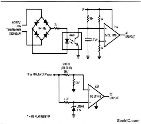
This circuit provides an indication if either or both the ac (line) or dc power to a digital system has dropped out. Fast ac-line dropout detection allows a memory-store command to be issued before dc power fails. Typically, the digital system regulators will continue to supply hold-up power for about 50 to 100 ms after ac-line dropout. This hold-up period (which should be verified in any individual application) permits adequate time to execute a memory-store operation. C1B serves as a final warning that power failure is imminent, by going low when the 5-V regulator drops below the threshold set by the selected resistors. These resistor values should be chosen so that C1B trips when the regulator input approaches the specified dropout voltage. (View)
View full Circuit Diagram | Comments | Reading(2043)
Analog voltage limiter circuit diagram
Published:2011/8/1 22:33:00 Author:Ecco | Keyword: Analog voltage limiter
View full Circuit Diagram | Comments | Reading(700)
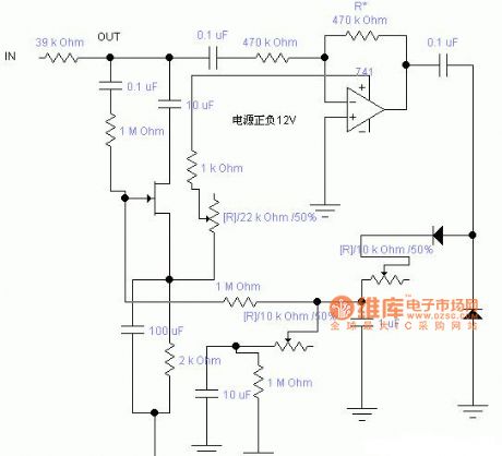
LOW_FREQUENCY_DOUBLER
Published:2009/7/4 20:59:00 Author:May
Signetics balanced modulator-demodulator transistor array is connected much like phase detector circuit.Output contains sum component which is twice frequency of input signal because same input signal frequency goes to both sections of balanced modulator.-Signetics Analog Data Manual, Signetics, Sunnyvale, CA, 1977, p 758. (View)
View full Circuit Diagram | Comments | Reading(0)
SIMPLE_DOUBLER_
Published:2009/7/4 20:53:00 Author:May
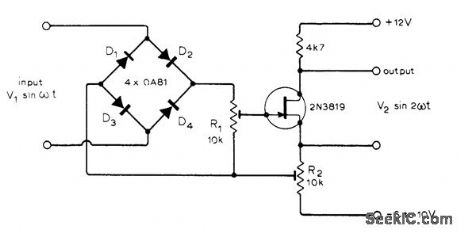
Performance is good up to about 10 kHz. R2 is adjusted to set FET just at cutoff under no-signal conditions, to give operation in square-law region. With R1correctly adjusted, using scope or third harmonic distortion monitor to obtain minimal distoltion, harmonic content of output can be made to approach that of sine-wave input. Article gives design equations.-R. Williams and J. Dunne, Frequency Doubler, Wireless World, Dec. 1975, p 575. (View)
View full Circuit Diagram | Comments | Reading(605)
CALL_ALERT
Published:2009/7/4 20:10:00 Author:May
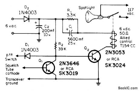
Developed to trigger relay when signal arrives at squelch tube in GE Progress Line 2-meter FM receiver. Relay is held energized about 2 s, determined by C1-R1, then deenergized for at least 25 s. Used for flashing red spotlight in room that is too noisy for hearing bell or buzzer. Circuit is easily adapted for any other FM receiver having squelch stage. Control circuit responds to small change in voltage at cathode of squelch tube. With no carrier present, tube conducts and places positive voltage at face of Q1, making it conduct and turn off Q2.When carrier arrives, Q1, restores bias to Q2, turning on relay. Connection to push-to-talk switch keeps lamp from flashing during transmission.-L. Waggoner, The WA0QPM Call Alert, CQ, May 1971, p 48-49 (View)
View full Circuit Diagram | Comments | Reading(991)
IF_AND_STEREO_DEMODULATOR
Published:2009/7/4 19:58:00 Author:May

National LM3089 IC and LM1310 PLL FM stereo demodulator provide all circuits required between FM tuner and inputs to power amplifiers of stereoreceivor Use of 10.7- MHz ceramic filters eliminates all but one IF alignment step. AFC output from pin 7 of IF strip drives center-tune meter.Wide bandwidth of detector and audio stage in IF strip is more than adequate for stereo receivers. Audio stage can be muted by input voltage to pin 5. Demodulator lC includes automatic stereo/monaural switching and l00-mA stereo indicator lamp driver. Optional 300-pF capacitor on pin 6 of LM3089 can be used to limit bandwidth.- Audio Handbook, National Semiconductor, Santa Clara, CA, 1977, p 3-18-3-23. (View)
View full Circuit Diagram | Comments | Reading(3391)
ANALOG_PLL_AS_FM_DEMODULATOR
Published:2009/7/4 19:42:00 Author:May

Upper frequency limit of about 50 MHz for NE562 and other monolithic analog phase-locked loops complicates construction of FM telemetry receivers that directly demodulate standard 88-108 MHz FM broadcast signals. Circuit shown solves problem, with only small amount of signal preconditioning, by first converting RF carrierto 10.7 MHz with conventional superheterodyne front end, then applying signal to phase detector of PLL with VCO set to run free at 10.7 MHz. Input sensitivity is less than 30 μV, and audio output is greater than 100 mV.-E. Murthi, Monolithic Phase-Locked Loops-Analogs Do All the Work of Digitals, and Much More, EDN Magazine, Sept. 5, 1977, p 59-64. (View)
View full Circuit Diagram | Comments | Reading(1972)
21_75MHz_DIODE_RECEIVER
Published:2009/7/4 5:31:00 Author:May
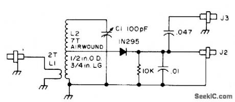
Covers 6-meter band and most 2-meter FM receiver oscillators near 45 MHz. Circuit is essentially that of crystal detector. Jack J3 gives AF output, and J2 gives DC output for meter.-B. Hoisington, Tuned Diode VHF Receivers, 73 Magazine, Dec. 1974, p 81-84. (View)
View full Circuit Diagram | Comments | Reading(1096)
Parallel_power_RS_232_transceivers
Published:2009/7/23 22:20:00 Author:Jessie
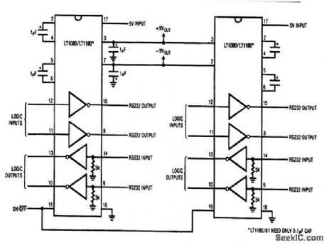
This circuit shows two LT1080 RS-232 transceivers operated from 5-V power. Twice the output current is available for external use. Also, the circuit produces ±9-V power output, as needed. The circuit eliminates two capacitors, although individual charge-pump capacitors are still needed on each device. (View)
View full Circuit Diagram | Comments | Reading(488)
Simple_RF_leveling_loop
Published:2009/7/23 22:19:00 Author:Jessie
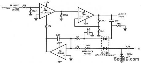
This circuit stabilizes the amplitude of an RF signal against variations in input, time, and temperature. A1 (an OTA, chapter 11) feeds current-feedback amplifier A2. The A2 output is sampled by the A3-biased gain-control configura-tion. The 4-pF capacitor compensates rectifier diode capacitance, which enhances output flatness versus frequency. The A1 ISET input current controls A1 gain, and allows overall output-level control. (View)
View full Circuit Diagram | Comments | Reading(646)
ZERO_ORDER_DATA_HOLD
Published:2009/7/23 22:19:00 Author:Jessie
Samples analog signal and holds sample value for period much longer than sampling aperture, as required in some sampled data systems and analog-to-digital converters. Used to sample inputs to accuracy of 0.1% of full scale, using sampling aperture greater thorn 1.25 microsec. Value of C is equal to sampling aperture divided by resistance in charge and discharge path.-E. Nelson, Zero. Order Data Hold, FEE, 11:7, p 26-27. (View)
View full Circuit Diagram | Comments | Reading(817)
TONE_PROBE_FOR_TESTING_DIGITAL_ICs
Published:2009/7/3 5:28:00 Author:May
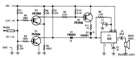
Circuit Notes
The tone probe uses sound to tell the status of the signal being probed. The probe's input circuit senses the condition of the signal and produces either a low-pitched tone for low-level signals (less than 0.8 V) or a high-pitched tone for high-level signals (greater than 2 V). (View)
View full Circuit Diagram | Comments | Reading(1771)
CLOCK_DRIVER
Published:2009/7/3 5:25:00 Author:May
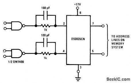
Circuit uses National DS0026CN monolithic clock driver as directcoupled driverfor address or precharge lines on MM1103 RAM at frequencies above 1 MHz. Can be driven by standard TTL gates and flipflops.- Memory Databook, National Semiconductor, Santa Clara, CA, 1977, p 11-27-11-36. (View)
View full Circuit Diagram | Comments | Reading(657)
Memory_save_at_power_down
Published:2009/7/23 22:19:00 Author:Jessie
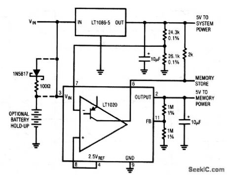
This dc-sensing circuit is useful where ac-line dropout (Fig. 6-54) is not feasible. The circuit uses the different dropout voltages of two regulators. When VIN input power (which could be from a battery or filter capacitor) falls, the LT1086 drops out first. This is detected by the LT1020 comparator, which goes low to alert the memory section (MEMORY STORE). The LT1020 regulator output maintains memory power for additional time, but finally begins to fall about 50 ms after the MEMORY STORE command. The optional connections shown allow extended hold-up times. (View)
View full Circuit Diagram | Comments | Reading(590)
PROM_PROGRAMMER
Published:2009/7/3 5:23:00 Author:May
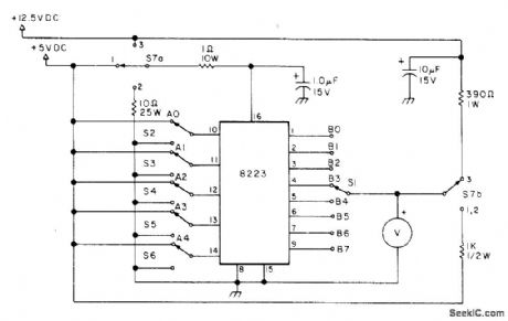
Can be used to blow links one by one, as required, on 8223 programmable read-only memory and on 82S23 Schottky version. Article covers construction, pretesting, and operation.-R. M. Stevenson, An 82S23 PROM Programmer!, 73 Magazine, June 1977, p 82-83. (View)
View full Circuit Diagram | Comments | Reading(2158)
512_BIT_PROM_PROGRAMMER
Published:2009/7/3 5:20:00 Author:May
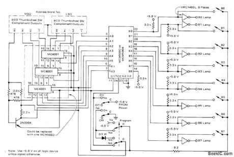
SimpIe manual programmer requires minimum equipment for fusing memory links of Motorola MCM5003 or MCM5004 programmable read-only memory.One link is fused at a time. MC1489 quad line receivers show contents of output bits by driving 5-V 20-mA lamps. Address word number is selected with two BCD thumbwheel switches.Three MC4001 ROMs convert BCD code to that required at address inputs. Program/verify switch must simultaneously be set along withproper output switch for each used bit.-J.E.Prioste, Programming the,MCM5003/5004 Programmable Read Only Memory, Motorola,Phoenix.AZ,1974,AN-550,p4 (View)
View full Circuit Diagram | Comments | Reading(1831)
RS_232_transceiver_operated_from__12__and__5_V_power_with_9_V_output
Published:2009/7/23 22:22:00 Author:Jessie

This circuit is useful in PCs where both + 12 V and + 5 are available. The +12 V is connected into one of the charge-pump capacitor pins, rather than the 12V output pin. Supply current decreases to about 9 mA, and -9 V output is available at pin 7. (View)
View full Circuit Diagram | Comments | Reading(511)
FORWARD_CURRENT_BOOSTER
Published:2009/7/3 5:16:00 Author:May
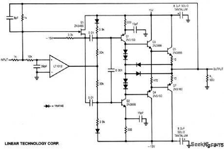
The LT1012 corrects dc errors in the booster stage, and does not set high-frequency signals. Fast signals are fed directly to the stage via Q5 and the 0.01-μF coupling capacitors. Dc and low-frequency signals drive the stage via the op-amp's output. The output stage consists of current sources, Q1 and Q2, driving the Q3 - Q5 and Q4 - Q7 complementary emitter follows. The diode network at the output steers drive away from the transistor bases when output current exceeds 250 mA, providing fast short-circuit protection. The circuit's high frequency summing node is the junction of the 1-K and 10-K resistors at the LT1012. The 10 K/39 pF pair filters high frequencies, permitting accurate dc summation at the LT1012's positive input. This current-boosted amplifier has a slew rate in excess of 1000 V/μS, a full power bandwidth of 7.5 MHz and a 3-dB point of 14 MHz. (View)
View full Circuit Diagram | Comments | Reading(566)
| Pages:277/471 At 20261262263264265266267268269270271272273274275276277278279280Under 20 |
Circuit Categories
power supply circuit
Amplifier Circuit
Basic Circuit
LED and Light Circuit
Sensor Circuit
Signal Processing
Electrical Equipment Circuit
Control Circuit
Remote Control Circuit
A/D-D/A Converter Circuit
Audio Circuit
Measuring and Test Circuit
Communication Circuit
Computer-Related Circuit
555 Circuit
Automotive Circuit
Repairing Circuit