
Basic Circuit
Index 270
FAST_15_V_BLINKER
Published:2009/7/5 23:28:00 Author:May
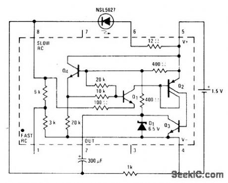
Addition of 1K resistor between pins 4 and 8 of National LM3909 IC in creases flash rate to about 3 times that obtainable when 300 μF is connected between pins 1 and 2. Modification of external connections gives choice of 3K, 6K, or 9K for internal RC resistors.- Linear Applications, Vol, 2, National Semiconductor, Santa Clara, CA, 1976, AN-154 ,p 2.
(View)
View full Circuit Diagram | Comments | Reading(492)
D_A_converter_with_0__to__10_V_unipolar_voltage_output
Published:2009/7/23 21:54:00 Author:Jessie
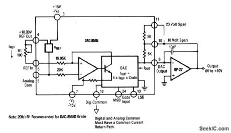
This circuit shows a DAC/op-amp combination that is used to provide a 0- to +10-V unipolar output. Pin 8 should be grounded if it is not used for trimming. To calibrate, turn all bits on (+5 V) and adjust R1 until the output is +9.9976 (full scale should be adjusted to 1 LSB less than +10.000V).If +10.2375V full scale is desired (exactly 2.5 mV/bit), insert a 120-Ω resistor in series with the gain resistor at pin 10 to the Op-amp output. If a 0- to a +5-V output is desired, tie pin 11 to pin 9, rather than to pin 10, and adjust the full scale to +4.9988 V. (View)
View full Circuit Diagram | Comments | Reading(720)
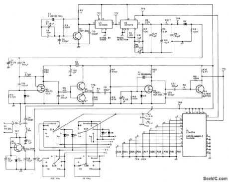
146000_147995_kHz_SYNTHESIZER_1
Published:2009/7/5 23:26:00 Author:May

Designed for use with Drake TR-33C transceiver.Circuit has built-in offset providing choice of any 5-kHz-spaced channl in frequency range for transmit and receive frequencies. Only two crystals are required. Desired frequency can be entered with BCD thumbwheel switches. Tuneup and testing procedures are given. Dt is 1N5530, D2 is 1N5144, and other diodes can be 1N914 or equivalent. Unmarked bipolar transistors are fast-switching silicon types; NPNs can be 2N2222, and PNPs can be 2N4403.-J. Moell, Super Deluxing the TR-33, 73 Magazine, April 1978, p 72-74. (View)
View full Circuit Diagram | Comments | Reading(1631)
SINGLE_POT_WlEN
Published:2009/7/5 23:23:00 Author:May
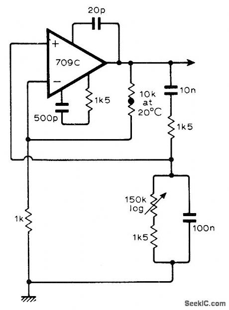
Can be tuned from 340 to 3400 Hz with single 150K Iogarithmic pot. Output is constant over tuning range. Opamp can also be 741. Components in the two arms of the Wien bridge have Iarge ratio to each other, so attenuation of network is only slightly affected by changein one of resistors.-P. C. Healy,Wien Oscillator with Single Component Frequency Control, Witeless World, Aug. 1974. p 272. (View)
View full Circuit Diagram | Comments | Reading(567)
12_V_FLUORESCENT
Published:2009/7/5 23:21:00 Author:May
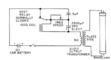
Relay acts as mechanical DC/AC converter operating off 12-V car battery.Each time relay opens, inductive kick in relay coil is stepped up by outputtransformerto high enough voltage for ionizing 24-inch fluorescent tube, giving flash that can serve as emergency flasher when car breaks down.-Circuits, 73 Magazline, June 1975, p 175.
(View)
View full Circuit Diagram | Comments | Reading(1029)
146000_147995_kHz_SYNTHESIZER
Published:2009/7/5 23:19:00 Author:May
Designed for use with Drake TR-33C transceiver Circuit has built-in offset providing choice of any 5-kHz-spaced channel in frequency range for transmit and receive frequencies. Only two crystals are required. Desired frequency can be entered with BCD thumbwheel switches. Tuneup and testing procedures are given. D1 is 1N5530, D2 is 1N5144, and other diodes can be 1N914 or equivalent. Unmarked bipolar transistors are fast-switching silicon types; NPNs can be 2N2222, and PNPs can be 2N4403.-J. Moell, Super Deluxing the TR-33, 73 Magazine, April 1978, p 72-74. (View)
View full Circuit Diagram | Comments | Reading(714)
PHASE_SHIFT_SINE_WAVE
Published:2009/7/5 23:19:00 Author:May
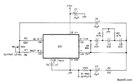
Uses NE571 analog compandor as phase-shift oscillator, with internal inverting amplifier serving to sustain oscillation. C1, C2, and C3 are timing capacitors, while R1 and R2 serve for phase-shift network.Suitable for use only as spot-frequency AF oscillator, with frequency being varied by changing values of C1, C2, and C3. Total harmonic distortion is only 0.01% at 3-V output.-W.G.Jung, Gain Control IC for Audio Signal Processing, Ham Radio, July 1977, p 47-53. (View)
View full Circuit Diagram | Comments | Reading(1787)
600_kHz_OFFSET_
Published:2009/7/5 23:18:00 Author:May
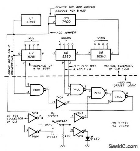
Developed for use with GLB400B frequency synthesizer which uses programmable divider and has outputs available from each flip-flop. Requires only two ICs, shown below horizontal dashed line. Select higher frequency of repeater pair on frequencyset switches. For operation at 146-147 MHz, select offset Tx to transmit on repeater input. For 147-148 MHz, select offset Rx to receive on repeater output. To operate in reverse, flip switch to other position, At center-off position, both transmit and receive are on selected frequency, with offset function disabled. LED lights only for offset.-D. Sargent, 600 kHz Offset for Frequency Synthesizers, Ham Radio, July 1978, p 98. (View)
View full Circuit Diagram | Comments | Reading(1120)
FLIP_FLOP_DRIVES_SCR
Published:2009/7/5 23:17:00 Author:May
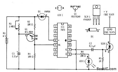
UJT relaxation oscilllator al serves as clock for driving section of 7473 dual flip-flop,One output of flip-flop-flashes Radio Shack 276-041 red LED to indicate operating status,Other output alternately triggers SCR which can be 6-A 50-V 276-1089,for COMPARATOR LED FLASHER-One section of LM339 quad comparator drives two RS2016 NPN transistors having LED load, to give simple flasher for classroom demonstrations. Circuit can be duplicated with other three sections to give four flashers. Connecting R2 to pin 1 of IC flashing lamp load. Load and SCR supply voltage depend on application but must be within SCR rating.-F. M. Mims, Semiconductor Projects,Vol. 2, Radio Shack,FortWorth,TX, 1976, p 62-70. (View)
View full Circuit Diagram | Comments | Reading(2612)
20_20000_Hz_LOW_DISTORTION
Published:2009/7/5 23:15:00 Author:May
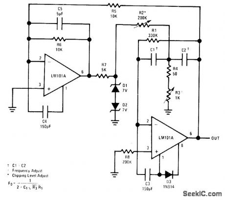
Opamp at right is driven by dquare-wave output of comparator at left, with feedback between opamps providing oscillation. Frequency range covered by tuning control R3 is determined by equalvalue capacitors C1 and C2, which range from 0.4 μF for 18-80 Hz to 0.002 μF for 4.4-20 kHz. Distortion rangesfrom 0.2% to 0.4% when 20% clipping of sine wave is provided by zeners.Both positive and negative supplies should be bypassed with 0.1-μF disk ceramic capacitors.- Easily Tuned Sine Wave Oscillators, National Semiconductor, Santa Clara, CA, 1971, LB-16. (View)
View full Circuit Diagram | Comments | Reading(605)
ALTERNATING_RED_GREEN
Published:2009/7/5 23:11:00 Author:May
National LM3909 IC is connected as relaxation oscillator for flashing red and green LEDs alternately. With 12-VDC supply, repetition rate is about 2.5 Hz.Green LED should have its anode or positive lead toward pin 5 as shown for lower LED, where shorter but higher-voltage pulse is available. LED types are not criticaL- Linear Applications, Vol. 2, National Semiconductor, Santa Clara, CA, 1976, AN-154, p 3. (View)
View full Circuit Diagram | Comments | Reading(572)
PHASE_INDICATOR
Published:2009/7/5 23:11:00 Author:May

The circuit provides a simple means of determining the succession of phases of a 3-phase 120 V source used in synchro work. Terminals A, B, and C are connected to the three terminals of the source to be checked. If the neon bulb lights, interchange any two leads; the light then extinguishes and A, B, and C indicate the correct sequence.
If power on any one line is lost, the neon bulb will light. This feature may be useful for monitoring purposes. (View)
View full Circuit Diagram | Comments | Reading(1344)
RC_CIRCUIT_DETECTS_PHASE_SEQUENCE_REVERSAL
Published:2009/7/5 23:10:00 Author:May
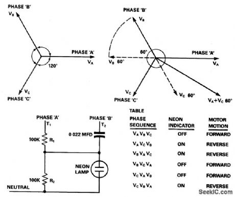
Assume the correct phase sequence to be VA-VB-VC. The circuit terminals are connected such that T1 gets connected to phase A and T2 to phase B. The capacitor advances the voltage developed across R2 due to phase B by - 60°, while the voltages developed across it by phase A is in phase with VA as shown in Fig. 69-1. The net voltage developed across R2~zero, the neon lamp is not energized, thereby signaling correct phase sequence. If terminal T2 gets connected to phase C, a large voltage, K(VA + VC60°), gets developed across R2, energizing the neon indicator to signal reverse phase sequence.
The motor terminals can be connected to the three phases in six different combinations. A three-phase motor will run in the forward direction for three such combinations, while for the other three it will operate in the reverse direction. As shown in the table, the circuit detects all three reverse combinations. This circuit can be wired into any existing motor starter where the operator can see whether the phase sequence has been altered, before starting the machine. (View)
View full Circuit Diagram | Comments | Reading(1607)
05_s_TONE_BURSTS
Published:2009/7/5 23:09:00 Author:May
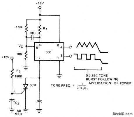
Simple 566 function generator circuit supplies audio tone for 0.5 s after power is applied, for use as communication-network alert signal. SCR is gated on when C2 charges up to its gate voltage, which takes 0.5 s, to shunt timing capacitor between pin 7 and ground and thereby stop tone. If SCR is replaced by NPN transistor, tone can be switched on and off manually at transistor base terminaL- Signetics Analog Data Manual, Signetics, Sunnyvale, CA, 1977, p 852-853. (View)
View full Circuit Diagram | Comments | Reading(711)
DEMONSTRATION_FLIP_FLOP
Published:2009/7/5 23:07:00 Author:May

Two sections of LM3900 quad opamp form bistable MVBR for flip-flop having two stable states. When input is grounded momentarily, output of one of opamps swings completely on and turns other opamp off. LED indicates which opamp is on at any particular time. Next grounding of input re verses conditions. Ideal for classroom demonstrations.-F. M. Mims, Integrated Circuit Projects, Vol. 5, Radio Shack, Fort Worth, TX, 1977, 2nd Ed., p 30-37. (View)
View full Circuit Diagram | Comments | Reading(2216)
SCOPE_CALIBRATOR
Published:2009/7/5 23:05:00 Author:May

The calibrator operates on exactly 100 kHz providing a reference for calibrating the variable time base oscillator of general purpose scopes. For example, if the scope is set so that one cycle of the signal fills exactly 10 graticule divisions then each division represents 1 MHz, or 1 microsecond. If the scope is adjusted for 10 cycles on 10 graticule divisions. (1 cycle per division) then each division represents 100 kHz or 10 microsecends. (View)
View full Circuit Diagram | Comments | Reading(1775)
SEQUENTIAL_SWITCHING_OF_LOADS
Published:2009/7/5 23:01:00 Author:May

Ring counter using four-layer diodes DN provides sequential switching of loads under control of input pulse-train signal. Indicator lamps are shown, but any load from 15 to 200 mA can be switched. After power is applied, reset switch must be pressed to establish current through L.When switch is released, this current fiows through C2 and breaks down D2, allowing current to flow through first lamp I1. Input pulse to transistol Q (normally held off by current through R1)turns Q off and removes power from diode circuits, thus turning I1 and D2 off. At end of input pulse, a comes on and restores power to diode circuits, but all loads will be turned off.Voltage on C3 now adds to 6 V normally across D4, making D4 break down and turn on I2. Next input pulse will breakdown D6 in same manner.Output signals may be picked up as negative pulses at A or B or by current-sensing at C if required for controlling larger loads,-J. Bliss and D. Zinder, 4-Layer and Current-Limiter Diodes Reduce Circuit Cost and Comptexity, Motorola, Phoenix, AZ, 1974, AN-221, p 5.
(View)
View full Circuit Diagram | Comments | Reading(683)
ANALOG_MULTIPLEXER_CONVERTS_SINGLE_TRACE_SCOPE_TO_FOUR_TRACE
Published:2009/7/5 23:01:00 Author:May
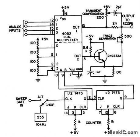
This adapter circuit, based on a dual four-channel analog multiplexer handles digital signals to at least 1 MHz, and analog signals at least through the audio range. The dual multiplexer's upper half selects one input for display. The lower half generates a staircase to offset the baselines of each channel, keeping them separate on the screen. The emitterfollower buffers the staircase, which is then summed with the selected signal. A two-bit binary counter addresses the CMOS 4052 multiplexer. (View)
View full Circuit Diagram | Comments | Reading(3051)
PCD3320P/PCD3326D Microcomputer Dialing Integrated Circuit
Published:2011/7/28 23:11:00 Author:Michel | Keyword: Microcomputer Dialing, Integrated Circuit


PCD3320P/PCD3326D is the microcomputer dial-up integrated circuit produced by Dutch Philips Company , and it is used in communication equipment and pulse dial-up circuit.
PCD3320P/PCD3326D integrated circuit contains pulse dial-up generating and key switch decoding circuits etc.This circuit adopts feet 18 DIP package and its pins functions and data are shown as the table 1.
Table 1:Pins Fuctions and Data of PCD3320P/PCD3326D IC (View)
View full Circuit Diagram | Comments | Reading(747)
Unipolar_D_A_converter
Published:2009/7/23 21:49:00 Author:Jessie
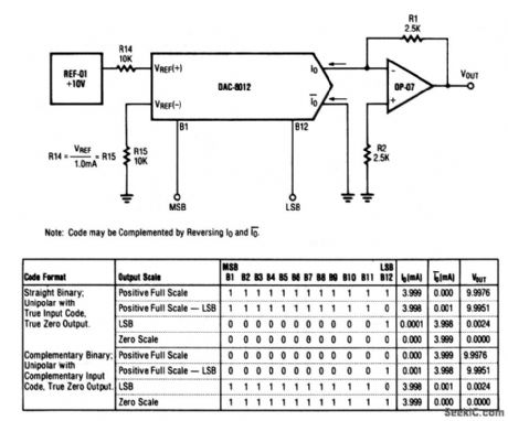
This circuit shows a DAC/op-amp combination that is used to provide unipolar positive-reference D/A converter operation. Full-scale adjustment can be made as shown in Fig. 6-39B. (View)
View full Circuit Diagram | Comments | Reading(510)
| Pages:270/471 At 20261262263264265266267268269270271272273274275276277278279280Under 20 |
Circuit Categories
power supply circuit
Amplifier Circuit
Basic Circuit
LED and Light Circuit
Sensor Circuit
Signal Processing
Electrical Equipment Circuit
Control Circuit
Remote Control Circuit
A/D-D/A Converter Circuit
Audio Circuit
Measuring and Test Circuit
Communication Circuit
Computer-Related Circuit
555 Circuit
Automotive Circuit
Repairing Circuit