
Basic Circuit
Index 274
PICTURE_DRAWING_LIGHT_PEN
Published:2009/7/5 21:54:00 Author:May
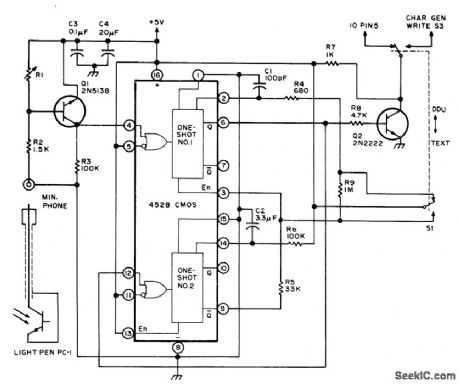
Circuit improves ability to draw pictures on display screen with light pen by using short data lockout period to avoid smearing. Value of R1 depends on light pen; use 1 megohm for Texas lnstruments H-35. One-shot No. 1 produces constant-amplitude 200-ns pulse for storing 1 or 0 bit in 2102 memory of CRO graphics interface, One-shot No. 2 delays generation of another write command 0.25 s, giving operator time to withdraw or move pen before double dot is formed. R4 and C1 control length of writepulse, while R5 and C2 control wait time.-S. S.Loomis, Let There Be Light Pens, BYTE, Jan.1976, p 26-30. (View)
View full Circuit Diagram | Comments | Reading(1096)
D_A_converter_with_bipolar_output
Published:2009/7/23 21:58:00 Author:Jessie
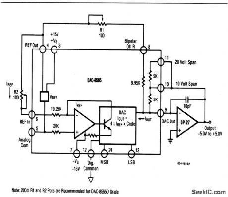
This circuit shows a DAC/op-amp combination that is used to provide ±5-V, ±10-V, or ±2.5-V bipolar outputs, with positive full-scale occurring when all bits are on (all 1s). To calibrate, turn off all bits, adjust R1 for -5.000, -10.000 or -2.500 V, depending on the range. If a precision op amp, such as the OP-27, OP-7, or OP-37 is used, no separate trimming of the op amp is required or recommended. (View)
View full Circuit Diagram | Comments | Reading(454)
_ADDRESS_STATE_ANALYZER
Published:2009/7/5 21:44:00 Author:May
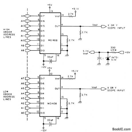
Dynamic fluctuations of 16-bit memory address bus are dis played on CRO for troubleshooting. Two MC1408 8-bit DACs drive inputs of CRO with analog equivalents of eight high-order and eight low-order address lines. Display serves as visual picture of computer in action, in which accessing of unexpected memory locations is instantly visible. Incoming address lines can be connected to MC1408s in any order. Article covers evaluation of scope patterns.-S. Ciarcia, A Penny Pinching Address State Analyzer, BYTE, Feb. 1978, p 6, 8, 10, and 12. (View)
View full Circuit Diagram | Comments | Reading(651)
DC_SERVO_DRIVE_EMPLOYS_BIPOLAR_CONTROL_INPUT
Published:2009/7/5 21:41:00 Author:May
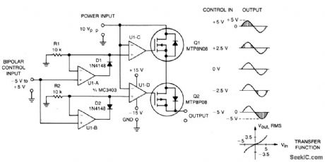
This circuit accepts bipolar control inputs of ±5 V and provides a phase-chopped output to a dc load (such as a servo motor) of the same polarity as the input. The rms voltage of the output is closely proportional to the control input voltage.
N-channel and p-channel TMOS devices, Q1 and Q2, are connected in anti-series to form a bidirectional switch through which current can flow in either the forward or reverse direction. Control circuits turn Q1 and Q2 on when they are reverse biased, bypassing their reverse rectif er and increasing circuit efflciency. Each device is allowed to turn off only when forward biased.
The Q1-Q2 switch connects the ac power source to the load when its instantaneous voltage is the same polarity and less than the control voltage. U1a is conftgured as an ideal positive rectifter whose output follows the control voltage when it is positive, and is zero otherwise. Similarly, U1b is a negative rectifier. U1c tums Q1 on whenever the ac input voltage is lower than the positive rectifier output. For negative control voltages, Q1 is turned on only during the negative half-cycle. For positive control voltages, Q1 is tumed on during the end portions of the positive half-cycle. Similarly, U1d turns Q2 on whenever the ac input voltage is higher than the output of the negative rectifier. (View)
View full Circuit Diagram | Comments | Reading(822)
VSUBPP_SUB_handshake_circuit
Published:2009/7/23 22:11:00 Author:Jessie
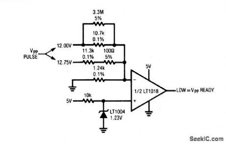
This circuit verifies that the VPP pulse generators (Figs. 6-49 and 6-50) are producing the correct output before pulsing begins. This is done by comparing the VPP output against the LT1004 reference. The LT1016 output goes low if the VPP output is correct. The resistor values shown allow for possible variations in VPP voltage because of component-tolerance stack-up. The output of the VPP generator should be set within 0.4% of nominal value when using this circuit. This can be done by trimming, or using 0.05% resistors in place of the 0.1% units specified. (View)
View full Circuit Diagram | Comments | Reading(533)
VOLTAGE_CONTROLLED_ATTENUATOR
Published:2009/7/5 21:37:00 Author:May
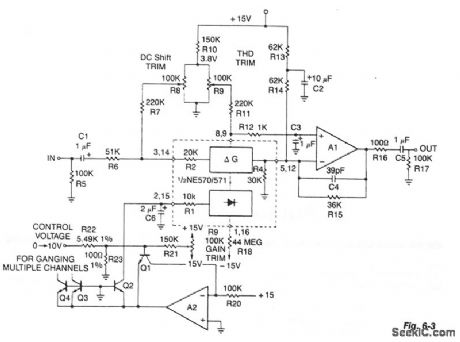
This typical circuit uses an external op amp for better performance and an exponential converter to get a control characteristic of -6 dB/V. Trim networks are shown to null out distortion and dc shift, and to fine trim the gain to 0 dB with 0 V of control voltage. (View)
View full Circuit Diagram | Comments | Reading(0)
PROGRAMMABLE_ATTENUATOR
Published:2009/7/5 21:35:00 Author:May
This circuit performs the function of dividing the input signal by a selected constant (1, 2, 4, 8, etc.).While T, Z, or L sections could be used in the input attenuator, this is not necessary since the amplifier loading is negligible and a constant input impedance is maintained. The circuit is thus much simpler and more accurate than the usual method of constructing a constant impedance ladder, and switching sections in and out with analog switches. Two identical circuits can be used to attenuate a balanced line. (View)
View full Circuit Diagram | Comments | Reading(454)
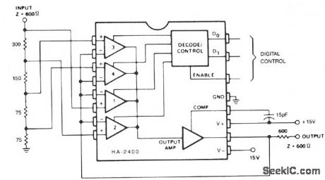
DIGITALLY_PROGRAMMABLE_ATTENUATOR_
Published:2009/7/5 21:34:00 Author:May

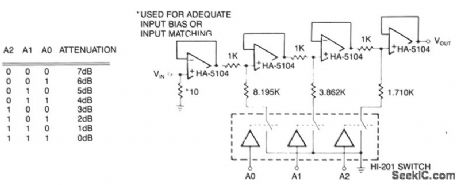
The first stage is a simple buffer used to isolate the signal source from the attenuator stages to follow. Each of the subsequent stages is preceded by a voltage divider formed by two resistors and CMOS switch. Provided that the CMOS switch for each stage is closed, the drive signal will be attenuated according to the basic voltage divider relationship at each stage. In the event a switch is open, nearly all of the signal strength will be passed to the next stage through the 1-KΩ resistor. The amplifiers act as buffers for divider networks and reduce the interaction between stages. Eight levels of attenuation are possible with the circuit as illustrated, but more stages could be added. Each divider network must be closely matched to the resistor ratios shown or the level of attenuation will not match the levels in the logic chart. (View)
View full Circuit Diagram | Comments | Reading(614)
CURRENT_CONTROLLED_WlEN
Published:2009/7/5 21:32:00 Author:May
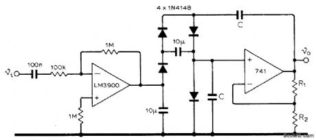
Small variations in input voltage to National LM3900 current-mode amplifier change frequency of fourdiode current-controlled Wien bridge over range from 10 to 50,000 Hz, with frequency being proportional to control current. Value of C is 700 pF. Ratio of R2 to sum of R1 and R2 should be greater than 3 to give voltage gain needed.-K. Kraus. Oscillator with Current-Controlled Frequency, Wireless World, Aug, 1974, p 272. (View)
View full Circuit Diagram | Comments | Reading(474)
Hitachi CMT2988 pincushion correction circuit
Published:2011/7/25 22:12:00 Author:Christina | Keyword: Hitachi, pincushion correction circuit
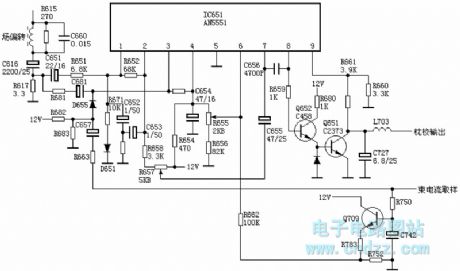
The 4V sawtooth wave voltage (peak-peak value) of the R617 adds to the pin-1 of IC651 through the C651 and R651, this voltage is amplified and disposed by the IC651, the pin-2 of IC651 outputs the 2V (peak-peak value) concave parabolic wave voltage, this voltage is integrated by the C653, C652 and R666, the R657 adjusts the amplitude of the parabolic wave, then it adds to the pin-7 of IC651 through the C655, it is amplified and reshaped by the IC651, the pin-8 outputs the convex parabolic wave voltage, this voltage is followed by the Q652's emitter and it is amplified by the Q651 to form the 9V (peak-peak value) concave parabolic wave voltage on both ends of C727.
(View)
View full Circuit Diagram | Comments | Reading(600)
SAA301OT Remote Transmitter Integrated Circuit
Published:2011/7/29 8:39:00 Author:Michel | Keyword: Remote Transmitter, Integrated Circuit

SAA301OT remote transmitter integrated circuit is widely used in video and audio system.
SAA30lOT contains integrated circuit keyboard switch decoding circuit and remote control launch carrier signal circuit, etc.This IC adopts feet 28 DIP package and its pins and data are shown as table 1.
Table 1 :SAA3010T IC Pind Functions and Data (View)
View full Circuit Diagram | Comments | Reading(725)
MEMORY_SAVE_ON_POWER_DOWN
Published:2009/7/5 21:28:00 Author:May
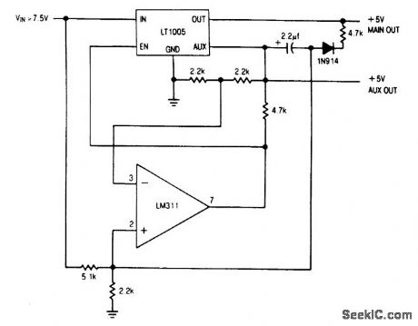
Circuit NotesThe auxiliary output powers the memory, while the main output powers the system and is connected to the memory store pin. When power goes down, the main output goes low, commanding the memory to store. The auxiliary output then drops out. (View)
View full Circuit Diagram | Comments | Reading(0)
INCREASING_THE_POWER_RATING_OF_ZENER_DIODES
Published:2009/7/5 21:27:00 Author:May
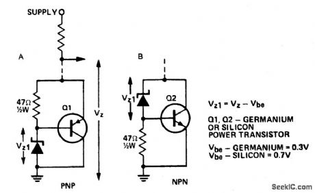
Circuit Notes
A power transistor can be used to provide a high powered zener voltage from a low wattage zener. A 400 mW zener can be used where a 10 watt zener is required or a 1W zener cait be used where a 50 to 80 watt zener is required by using appropriate transistors for Q1 and Q2 in the circuits shown. Where low rating is required, Q1 would be an ASZ 15 (germanium) or an AY9140 (silicon). Q2 could be a 2N2955 (silicon). For higher powers, Q1 should be an ASZ18 (germanium) or a 2N2955 (silicon) and Q2 a 2N3055 (silicon) or an AY8149 (silicon). A heatsink on the transistor is required. The circuit in A has the advantage that power transistors can be bolted directly on to a chassis which may serve as a heatsink. (View)
View full Circuit Diagram | Comments | Reading(0)
UPPERCASE_LOWERCASE_DRIVE_FOR_TV
Published:2009/7/5 21:25:00 Author:May
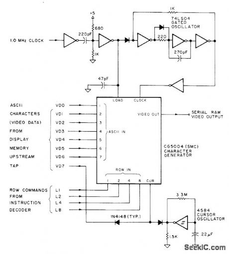
Standard Microsystems CG5004 alphamerle data-to-video converter provides both uppercase and lowercase characters and all numerals in serial video form for display as 7 x 9 character matrix on TV screen under microprocessor control. IC requires only single +5 V supply. Winking underline cursor is produced automatically by cursor oscillator. Internal shift register is part of IC. Raw video requires predistorting for clarity and addition of sync pulses before it can be fed to TV set.-D. Lancaster, TVT Hardware Design, Kilobaud, Jan. 1978, p 64-68. (View)
View full Circuit Diagram | Comments | Reading(653)
High_repetition_rate_VPP_programming_supply
Published:2009/7/23 22:05:00 Author:Jessie
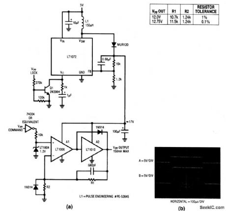
This circuit is similar to that of Fig.6-48, but with higher repetition rate, and with controlled rise time to eliminate overshoots (as shown in Fig.6-49B). (View)
View full Circuit Diagram | Comments | Reading(441)
AF_TONE_BURSTS
Published:2009/7/5 21:24:00 Author:May
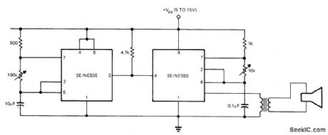
First 555 timer operates as slow astable multivibrator whose output is used to gate second timer operating as AF oscillator. Arrangement provides repeatable toneburst generation.-E. R. Hnatek. Put the IC Timer to Work in a Myriad of Ways. EDN Magazine. March 5. 1973. p 54-58. (View)
View full Circuit Diagram | Comments | Reading(508)
ZENER_DIODE_INCREASE_FIXED_PNP_REGULATOR’S_OUTPUT_VOLTAGE_RATINGS
Published:2009/7/5 21:23:00 Author:May
Circuit Notes
A zener diode in the ground lead of a fixed pnp regulator varies the voltage output of that device without a signiftcant sacriftce in regulation. The technique also allows the regulator to operate with output voltages beyond its rated limit. (View)
View full Circuit Diagram | Comments | Reading(0)
S18100D Switch Power Supply Thick-film Integrated Circuit
Published:2011/7/29 3:27:00 Author:Michel | Keyword: Switch, Power Supply, Thick-film, Integrated Circuit

S18100D is a kind of switch power supply thick-film integrated circuit that is widely used in Toshiba 219X6Y color TVs.
First,Functions FeaturesS18100D integrated circuit contains drive pulse output circuit, over-voltage and over-current protection circuit, standby control circuit and some other auxiliary functions circuit.
Second,Pins Functions and FeaturesS18100D IC adopts feet 11 package and its pins functions and data are shown as table 1.
Table 1:S18100D IC Pins Functions and Data (View)
View full Circuit Diagram | Comments | Reading(717)
Digitally_controlled_4__to_20_mA_current_loop_generator
Published:2009/7/23 22:14:00 Author:Jessie
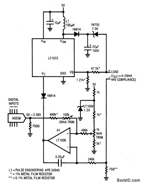
This 5-V circuit uses a servo-controlled dc/dc converter to generate the compliance voltage necessary for loop-current requirements in industrial-control (valves, etc.) applications. The circuit will drive 4 to 20 mA into loads as high as 2200 Ω (44 V compliance) and is inherently short-circuit protected. The digital input permits easy interface to digital systems. (View)
View full Circuit Diagram | Comments | Reading(937)
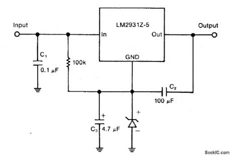
VOLTAGE_REGULATOR
Published:2009/7/5 21:21:00 Author:May

View full Circuit Diagram | Comments | Reading(2223)
| Pages:274/471 At 20261262263264265266267268269270271272273274275276277278279280Under 20 |
Circuit Categories
power supply circuit
Amplifier Circuit
Basic Circuit
LED and Light Circuit
Sensor Circuit
Signal Processing
Electrical Equipment Circuit
Control Circuit
Remote Control Circuit
A/D-D/A Converter Circuit
Audio Circuit
Measuring and Test Circuit
Communication Circuit
Computer-Related Circuit
555 Circuit
Automotive Circuit
Repairing Circuit