Basic Circuit
DIGITALLY_PROGRAMMABLE_ATTENUATOR_
Published:2009/7/5 21:34:00 Author:May | From:SeekIC


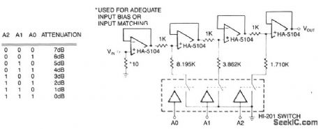
The first stage is a simple buffer used to isolate the signal source from the attenuator stages to follow. Each of the subsequent stages is preceded by a voltage divider formed by two resistors and CMOS switch. Provided that the CMOS switch for each stage is closed, the drive signal will be attenuated according to the basic voltage divider relationship at each stage. In the event a switch is open, nearly all of the signal strength will be passed to the next stage through the 1-KΩ resistor. The amplifiers act as buffers for divider networks and reduce the interaction between stages. Eight levels of attenuation are possible with the circuit as illustrated, but more stages could be added. Each divider network must be closely matched to the resistor ratios shown or the level of attenuation will not match the levels in the logic chart.
Reprinted Url Of This Article:
http://www.seekic.com/circuit_diagram/Basic_Circuit/DIGITALLY_PROGRAMMABLE_ATTENUATOR_.html
Print this Page | Comments | Reading(3)

Article Categories
power supply circuit
Amplifier Circuit
Basic Circuit
LED and Light Circuit
Sensor Circuit
Signal Processing
Electrical Equipment Circuit
Control Circuit
Remote Control Circuit
A/D-D/A Converter Circuit
Audio Circuit
Measuring and Test Circuit
Communication Circuit
Computer-Related Circuit
555 Circuit
Automotive Circuit
Repairing Circuit
Code: