
Basic Circuit
Index 278
ADDING_FOUR_FU_NCTlONS
Published:2009/7/3 5:12:00 Author:May
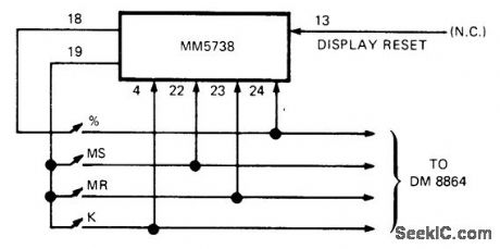
Capability of 8-digit four-function Novus 850 calculator made by National Semiconductor (also marketed as Montgomery Ward P50) can be doubled by adding four SPST swhches and connecting as shown. These provide additional functions of memory store, memory recall, percent, and constant. Switches can be put on front panel above display, at corners of battery. Cutler Hammer SA1BV20 SPST switches with SW53AA1 caps can be squeezed in.-D. Amett, Add Memory, Constant and % to a 4-Function Calculator, EDN Magazine, Aug. 20, 1975, p 82. (View)
View full Circuit Diagram | Comments | Reading(558)
TRANSISTOR_PUMP_DISCRIMINATOR
Published:2009/7/3 5:09:00 Author:May
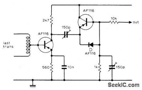
Used with 10.7-MHz IF strip of high-quality FM tuner built from discrete comDonents Circuit is placed between last IF stage and stereo decoder.-W. Anderson, F. M. Discriminator, Wireless World, April 1976, p 63. (View)
View full Circuit Diagram | Comments | Reading(695)
LEVEL_SHIFTER_FOR_RAM
Published:2009/7/3 5:09:00 Author:May
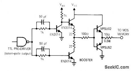
Uses predriverwith three transistors, followed by two-transistor booster, to convert TTL levels to those required by dynamic MOS random-access memory. Booster can be omitted for data input lines be-MEMORY cause they drive such low capacitive loads in typical arrays.-M. E Hoff, Designing an LSI Memory System That Outperforms Cores-Economically,Computer Hardware(section ofEDN Magazine), Jan 15, 1971, p 6-15(p000110-001111) (View)
View full Circuit Diagram | Comments | Reading(509)
LOW_PASS_PI_SECTION_AF
Published:2009/7/3 5:00:00 Author:May

Four-pole doublethrow switch gives choice of 650-Hz cutoff for CW or 2000 Hz for SSB.Filter capacitors are matched Response decreases continuously beyond cutoff frequency,with no loss of attenuation.-E.Noll,Circuits and Techniques,Ham Radio,April 1976,p 40-43. (View)
View full Circuit Diagram | Comments | Reading(780)
MEMORY_PROTECTING_REGU_LATOR
Published:2009/7/3 5:00:00 Author:May
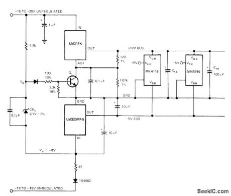
Developed for MOS RAM in which accidental removal of -5 V bias supply would allow buildup of currents flowing between +12 V and ground to value sufficient to open up metal paths and destroy memory. Protection is achieved by feeding unregulated negative voltage to on-card local regulator using LM320MP-5 to provide -5 V regulated bias for all memory chips. LM317K is used as +12 V regulator for delivering up to 1.5 A. If -12 V gradually drops out of regulation, a, turns on and pulls LM317K adjust pin to ground so output of this regulator drops to + 1.3 V and logic circuits are undamaged. If -12 V shorts to ground, capacitors on -5 V line hold up for several hundred microseconds so Q1 has time to turn off +12 V regulator. Use heatsinks for regulators.-R. Pease, Safe Supply Manages MOS Memories, EDNMagazine, Oct. 20, 1978, p 82 and 84. (View)
View full Circuit Diagram | Comments | Reading(576)
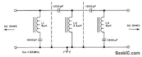
80_METER_BANDPASS
Published:2009/7/3 4:59:00 Author:May

Four-resonator filter for use in 80-meter amateur band has 100-kHz bandwidth, 4.4-dB insertion loss, and 6-60 dB shape factor of 5.16. Filter was designed and aligned at 3.75 MHz; realignment at 3.6 and 3.9 MHz yielded Similar results Artiole covers theory.construction, and adjustment-W Hay-ward,Bandpass Filters for Receiver Preselectors,Ham Radio,Feb,1975,p 18-27. (View)
View full Circuit Diagram | Comments | Reading(838)
SWITCHABLE_AF_FlLTER
Published:2009/7/3 4:58:00 Author:May

Provides wide range of switch-selected capacitor values for varying cutoff frequencies, to permit use of filter for either phone or CW reception. On CW, circuit improves reception by eliminating higher frequencies that are largely interference.-J. J.Schultz,The Quiet Maker, 73 Magazine, March 1974, p 81-84. (View)
View full Circuit Diagram | Comments | Reading(700)
AM_BROADCAST_REJECTlON
Published:2009/7/3 4:57:00 Author:May
Seven-element mderived high-pass filter provides 30-dB rejection at AM broadcast-band frequencies while passing signals in 160-meter band. Midsection Inderived branch of circuit was eliminated to simplify construction, but can be added and tuned to particular broadcast station that presents dffficult interference problem. L1 and L3 are 40 turns No. 30 enamel wound on T50-2 powderediron toroid. L2 has 22 turns No. 30 on T50-2 core.-D. DeMaw, Low-Noise Receiving Antennas, QST, Dec. 1977, p 36-39. (View)
View full Circuit Diagram | Comments | Reading(607)
693_2079_Hz_TUNABLE_NOTCH
Published:2009/7/3 4:56:00 Author:May

Requires only one tuning pot to cover entire frequency range.Developed for use in tunable narrow-band audio amplifier. Article gives design equations.Depth of notch is greater than 50 dB. Doubling capacitor values changes tuning range to 355-1028 Hz, while cutting values in half gives range of 1340-4110 Hz.-C. Hall, Tunable RC Notch Filter, Ham Radio, Sept. 1975, p 16-20. (View)
View full Circuit Diagram | Comments | Reading(635)
225_Hz_BANDPASS_RTTY
Published:2009/7/3 4:55:00 Author:May

Used ahead of Limiter in 170-Hz-shift RTTY receiving converter.Chebyshev mesh configuration with 0.1-dB ripple uses inductor to ground for sharpening lower skirt, with capacitive coupling for sharpening upper skirt, to give good symmetry for response curve. Capacitors should be high-Q ty low in frequency. Insertion loss is 6.6 dB and 3-dB bandwidth is 225 Hz, which makes mark and space tones only 1.5 dB down.-A. J. Klappenberger, A High-Performance RTTY Band-Pass Filter, QST, Jan. 1978, p 33. (View)
View full Circuit Diagram | Comments | Reading(588)
05MHz_WITH_20_DEVIATION_
Published:2009/7/3 4:45:00 Author:May
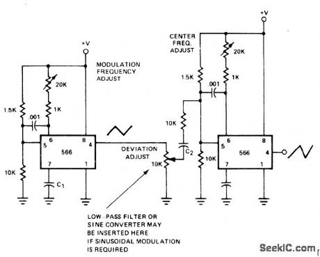
One 566 function generator serves for generating relatively low-frequency carrier (center frequency less than 0.5 MHz), and other 566 serves as modulator producing triangle output with frequency determined by C1. Combination is suitable for deviations up to ±20% of carrier frequency.- Signetics Analog Data Manual, Signetics, Sunnyvale, CA, 1977, p 852-853. I (View)
View full Circuit Diagram | Comments | Reading(569)
650_MHz_AMPLIFYING_PRESCALER_PROBE
Published:2009/7/3 4:44:00 Author:May
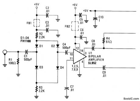
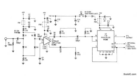
CircU1t Notes
The 650 MHz Prescaler Probe's input is terminated by resistor R1 and is fed through C1 to the diode limiter composed of D1 through D4. Those diodes are forward-biased by the + 5 volt supply for small-input signals and, in turn, feed the signal to U1. Howev-er, for larger input signals, diodes Dl through D4 will start to turn off, passing less of the signal, and, thus, attenuating it. But even in a full-off state, the FH1100-type diodes will always pass a small part of the input to U1 because of capacitive leakage within the diodes. Integrated circU1t U1, a Plessey SL952 bipolar amplifier, capable of 1 GHz operation, provides 20 to 30 dB of gain. The input signal is supplied to pin 10, U1 withthe other input (pin 11) is bypassed to ground. The output signal is taken at pin 3 and pin 4, with pin 3 loaded by R4 and pin 4 by R5.Integrated circU1t 11C90, U2, is a high-speed prescaler capable of 650 MHz operation configured for a divide-by-10 format. A reference voltage internally generated appears at pin 15 and is tied to pin 16, the clock input. This centers the capacitive-coupled input voltage from U1 around the switching threshold-voltage level. An ECL-to-TTL converter in U1 provides level conversion to drive TTL input counters by typing pin 13 low.Therefore, no external EOL to TTL converter is reqU1red at the pin 11 output. On the other hand, EOL outputs are available at U2, pin 8 (Q4) and at pin 9 (Q4), if desired.In that circU1t configuration, pin 13 is left open, and U2 will use less power. (View)
View full Circuit Diagram | Comments | Reading(3222)
Double-barreled single-block circuit diagram
Published:2011/8/1 21:21:00 Author:Ecco | Keyword: Double-barreled , single-block
The main transistor with resistance is a kind of small power tube, which is used as the electronic switch or inverter in household appliances and other electronic devices. Some band-stop tubes contain two transistors and lead 5-6 feet (dual-barreled single-resistance model, it is shown in Figure)
(View)
View full Circuit Diagram | Comments | Reading(473)
PLL_IF_AND_DEMODULATOR
Published:2009/7/3 4:40:00 Author:May
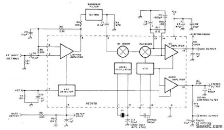
Signetics NE563B IC(In dashed lin es)serves as completeIF amplifier and demodulator for FM broadcastrecelver, Circuit uses downconversion from 10.7 MHz to 900 kHz, where phase detector operates. Ceramic bandpass filter provides IF selectivity at 10.7 MHz. X1 can be 9.8-MHz ceramic resonator, LC network, crystal, or capacitor.-H. Olson, FM Detectors, Ham Radio, June 1976, p22-29. (View)
View full Circuit Diagram | Comments | Reading(1777)
Simple_RS_232_receiver
Published:2009/7/23 22:27:00 Author:Jessie
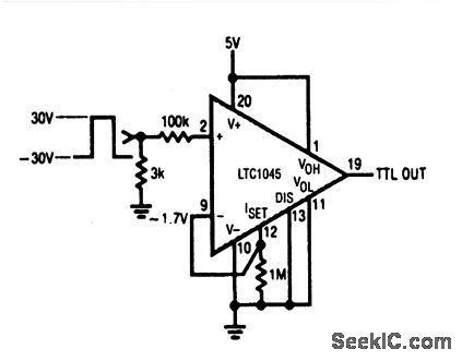
This circuit shows a simple way to build a battery-powered RS-232 receiver. The input voltage can be driven as much as ±30 V without adverse effects because the 100-kΩ resistor prevents device damage. With a 1-MΩ RSET resistor at pin 12, the LTC1045 draws only 100 μA of quiescent current, and has a propagation delay of 1.2 μs. Only a single 5-V supply is required. (View)
View full Circuit Diagram | Comments | Reading(703)
QUADRATURE_DEMODULATOR
Published:2009/7/3 4:32:00 Author:May
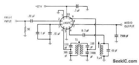
Quadrature coil associated with balanced-mixer demodulation system is connected to pin 6 of National LM373 IC, and output signal is taken from pin 7.Good output is obtained with only ±5 kHz deviation at either 455 kHz or 10.7 MHz. Can be operated as wideband or narrow-band circuit by choosing appropriate interstage and output LC and RC components.-E. M. Noll, Linear IC Principles, Experiments, and Projects, Howard W. Sams, Indianapolis, IN, 1974, p 350-351. (View)
View full Circuit Diagram | Comments | Reading(1660)
WAVE_SYNTHESlZER
Published:2009/7/3 4:31:00 Author:May
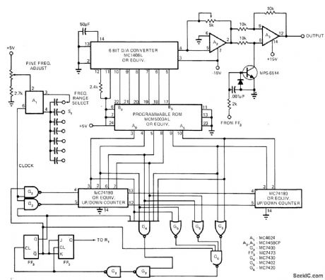
Virtually any symmetrical waveform can be generated by using only IC counters, a read-only memory, and a monolithic D/A converter. Only first 90 °of waveform need be digitized; this information can be manipulated to generate other 270 °and repeated as often as necessary. To digitize desired wave form, divide first 9O °into 64 points, calculate sine or other function for each, multiply each result by 63 to normalize, round off, convert each to 6-bit binary equivalent, take complements, and use results for programming ROM.Article describes operation of circuit in detail.Use of MC1480 8-b'ffi monolithic D/A converter gives better resolution than is possible with MC1406L 6-bit D/A converter because 8-bit words give 256 discrete output levels instead of 64.-K. Huehne, Programmable ROMs Offer a Digital Approach to Waveform Synthesis, EDN Magazine, Aug. 1, 1972. p 38-41. (View)
View full Circuit Diagram | Comments | Reading(588)
Isolated_data_acquisition_system
Published:2009/7/23 22:27:00 Author:Jessie

This circuit shows an 8-input LTC1090 data-acquisition IC connected to a system with 500-V isolation (provided by 4N28 opto-isolators). The number of channels can be increased to 16, 24, 32, etc, with one additional opto-isolator used to increase the number of channels in multiples of 8. Up to 24 channels can be powered directly by the LT1021. The circuit is capable of transferring serial data at about a 15-kHz rate. A code written for the Motorola 68HC05 processor is available from Linear Technology. (View)
View full Circuit Diagram | Comments | Reading(1954)
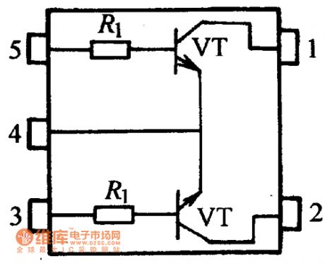
Double-barreled double-block circuit diagram
Published:2011/8/1 21:20:00 Author:Ecco | Keyword: Double-barreled , double-block
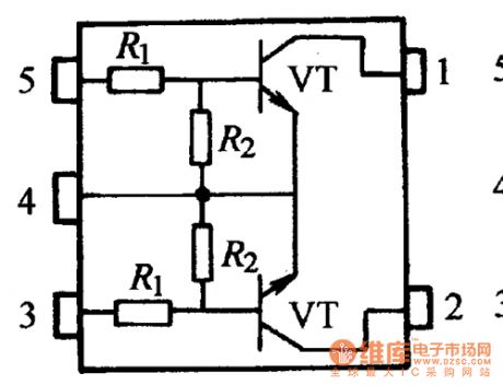
The main transistor with resistance is a kind of small power tube, which is used as the electronic switch or inverter in household appliances and other electronic devices. Some band-stop tubes contain two transistors and lead 5-6 feet (dual-barreled dual-resistance model, it is shown in Figure)
(View)
View full Circuit Diagram | Comments | Reading(444)
PROGRAMMING_OF_PROM
Published:2009/7/3 4:22:00 Author:May
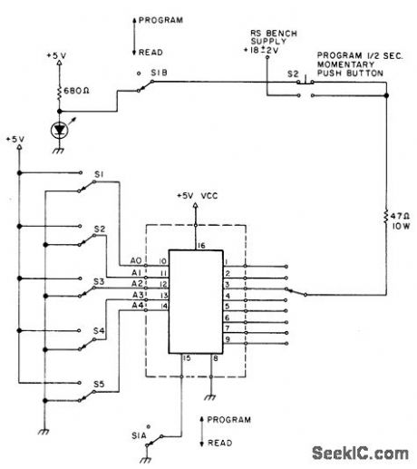
Simple circuit is effective for 82S23, DM8577, and 74188 PROMs.With DM8577, circuit changes logic 1s to 0s.With 82S23, 0s are changed to 1s. Set address switches for word to be programmed, set S1 to program position, set S3 to bit to be programmed, and push S2 momentarily (less than 0.5 s). To verify that bit has been programmed, return S1 to read position and observe LED.Supply can be three 6-V lantern batteries in series.-Ham Help, 73Magazine, April 1977, p 42. (View)
View full Circuit Diagram | Comments | Reading(2589)
| Pages:278/471 At 20261262263264265266267268269270271272273274275276277278279280Under 20 |
Circuit Categories
power supply circuit
Amplifier Circuit
Basic Circuit
LED and Light Circuit
Sensor Circuit
Signal Processing
Electrical Equipment Circuit
Control Circuit
Remote Control Circuit
A/D-D/A Converter Circuit
Audio Circuit
Measuring and Test Circuit
Communication Circuit
Computer-Related Circuit
555 Circuit
Automotive Circuit
Repairing Circuit