
Basic Circuit
Index 275
EEPROM_VSUBPP_SUB_pulse_generator
Published:2009/7/23 22:12:00 Author:Jessie

This circuit is similar to that for flash memories (Figs. 6-48, 6-49, and 6-50), but is designed specifically for EEPROMS. (View)
View full Circuit Diagram | Comments | Reading(738)
TRANSFORMERLESS_TONE_ANNUNCIATOR
Published:2009/7/5 21:21:00 Author:May

This circuit does not require an output transformer or an output coupling capacitor;the annunciator can easily be turned on or off by a control input voltage driving a 10-MΩ input resistor, R3. For a smaller acoustic output, replace output transistor, Q1, with a 100-Ω resistor, while also raising the voice coil impedance to 100Ω, to prevent loading of the IC. (View)
View full Circuit Diagram | Comments | Reading(1276)
SCR_PREREGULATOR_FITS_ANY_POWER_SUPPLY
Published:2009/7/5 21:20:00 Author:May

Circuit Notes
This SCR pre-regulator keeps the filter capacitor Vc, in a variable output power supply, a few volts above the output voltage Vo. The benefits include: less heat dissipated by the pass transistor and therefore small heatsink, cooler operation and higher efficiency, especially at low output voltages.Q1, R1, R2, D1 and D2 form a constant current source for zener Z1, so that the contribution to the output current is always a few mA (2-3 mA).The Darlington pair Q2, Q3 keeps the SCR off. The voltage Vcdecreases until Vc= Vo=V at which point the Darlington pair fires the SCR, charging the filter capacitor to a higher voltage Vc1 in less than half the period of the input voltage. The component values, shown are for a 0-250-V, 3-A power supply. (View)
View full Circuit Diagram | Comments | Reading(5567)
1_kHz_L0W_DISTORTlON
Published:2009/7/5 21:19:00 Author:May
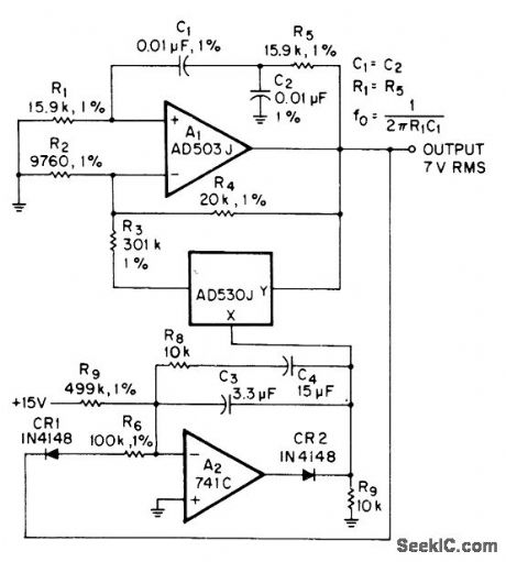
Total harrnonic distortion is only 0.01% in amplitude-stabilized oscillator delivering 7 VRMS. Opamp A1 has closed-loop gain of 3. Regenerative feedback through bandpass filter C1-C2-R1-R5 determines frequency of oscillation. Output is stabilized by multiplier whose control voltage is derived from integrator A2.-R. Burwen. Ultra Low Distortlon Oscillator. EDN/EEE Magazine. June 1. 1971. p 45. (View)
View full Circuit Diagram | Comments | Reading(426)
PROGRAMMED_BIT_RATES
Published:2009/7/5 21:12:00 Author:May
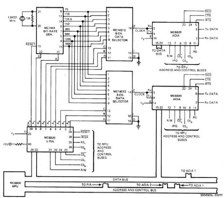
Choice of 37 differentbit rates in rangefrom 75 to 1800 b/s, each multiplied by 1, 8, 16, or 64, can be obtained from Motorola MC1441 bit-rate generator, two 8-channel data selectors, half of peripheral interface adapter (PIA) and two asynchronous communication interface adapters (ACIA) by appropriate programming of Motorola MC6800 microprocessor used in data communication system. Article gives operating details and example of Initialization program,-C,Nash,Microprocessor Software Programs Bit-Rate Generator,EDN Magazine.Aug 20.1977.p134.136.and 137. (View)
View full Circuit Diagram | Comments | Reading(1124)
OFF_LINE_FLYBACK_REGULATOR
Published:2009/7/5 21:10:00 Author:May
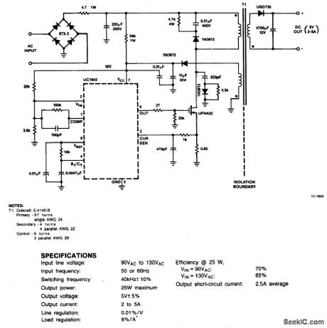
Circuit NotesThis circuit uses a low-cost feedback scheme in which the dc voltage developed from the primary-side control winding is sensed by the UC1842 error amplifier. Load regulation is therefore dependent on the coupling between secondary and control windings, and on transformer leakage inductance. For applications requiring better load regulation, a UC1901 Isolated Feedback Generator can be used to directly sense the output voltage. (View)
View full Circuit Diagram | Comments | Reading(0)
S7230B Microcomputer Dailing Integrated Circuit
Published:2011/7/29 0:40:00 Author:Michel | Keyword: Microcomputer, Dailing, Integrated Circuit

S7230B is microcomputer dailing integrated circuit and it is used in communication device and used as dailing circuit.
S7230B IC adopts feet 22 DIP package and its pins functions and data are shown as table 1.
Table 1:S7230B IC Pins Functions and Data (View)
View full Circuit Diagram | Comments | Reading(614)
S2569 Microcomputer Dialing Integrated Circuit
Published:2011/7/29 2:54:00 Author:Michel | Keyword: Microcomputer Dialing, Integrated Circuit

S2569 is produced by the British micro system company and it is widely used in communication equipment and dialing circuit.
2569 can produce 12 double audio signal and twelve keyboard correspondent position, which adds repeatation,stitches, pause and flashing functions.The IC has A, B and C series products, the feet 16 DIP package and its pins functions and data are shown as table 1.
Table 1:S2569 IC Pins Functions and Data (View)
View full Circuit Diagram | Comments | Reading(561)
PROM_PROGRAMMER_1
Published:2009/7/5 21:05:00 Author:May
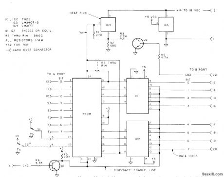
Developed specifically for programming Harris 7641-5 and 7681-5 PROMs, which come with logic 1 in all bit positions. Programmer is used to burn bit at each position requiring logic 0 by process equivalent to blowing fusible link on PROM chip. Process is not reversible, so one emor ruins PROM. Circuit uses two regulator ICs (IC3 and IC4) and two TTL gates (IC1 and IC2). Article gives programming procedure in detail. Software for generating critical timing and control signals with microprocessor is also given.-T. Hayek, Simple and Low-Cost PROM Programmer, Kilobaud, July 1978, p 94-96 and 98-99. (View)
View full Circuit Diagram | Comments | Reading(1796)
15_Hz_TO_150_kHz_IN_FOUR_RANGES
Published:2009/7/5 21:00:00 Author:May

Switch gives choice of ranges, with R2 and R3 varying frequency in each. Circuit draws only 4mA from two 9-V batteries and provides moderate output at 4-5 V. Connections shown are for TO-5 case of 741.-T. Schultz, Audio Oscillator. QST. Nov. 1974. p 43. (View)
View full Circuit Diagram | Comments | Reading(526)
PROGRAMMER_FOR_SCIENTIFIC_CALCULA_TOR
Published:2009/7/5 20:55:00 Author:May
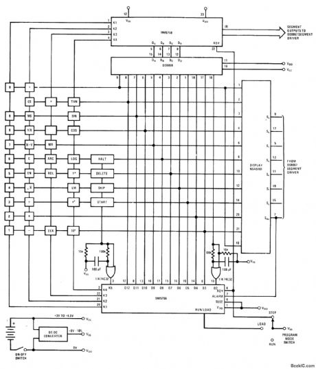
National MM5766 dynamic key sequence programmer can be added to MM5758 scientific calculator chip to provide learn-mode programmability. Cirouit memorizes any combination of key entries up to 102 characters while in load mode, then automatically plays back programmed sequence as often as desired in run mode. Halt key programs variable data entry points at which control is temporarily returned to operator in run mode.- MOS/LSl Databook, National Semiconductor, Santa Clara, CA, 1977, p 8-76-8-79. (View)
View full Circuit Diagram | Comments | Reading(732)
TEST_TONES
Published:2009/7/5 20:50:00 Author:May
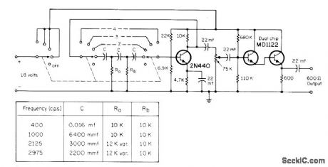
Provides preset frequencies of 400.1000.2125. and 2975 Hz Circuit consists of RC phase-shift oscillator driving Darlington emitter-follower that provides high-impedance load for osciIlator and stable 600- ohm output impedance.-s Kelly. A Simple Audio Test Oscillator.CQ1 Oct. 1970. p 50.and 90. (View)
View full Circuit Diagram | Comments | Reading(631)
DOUBLER_FOR_1_Hz_TO_12_MHz
Published:2009/7/5 20:49:00 Author:May

Simple arrangement of EXCLUSIVE-OR,mono,and hex Inverter ICs ρrovides extremely accurate frequency doubling in digital systems, along with waveform symmetry. Article gives design equation Series inverters create about 120 ns of .delay.-V. Rende, Frequency Doubler Operates from 1 Hz to 12 MHz, EDN Magazine, Aug. 20, 1976,p 85. (View)
View full Circuit Diagram | Comments | Reading(2362)
1_50_kHz_SINE_WAVE
Published:2009/7/5 20:43:00 Author:May
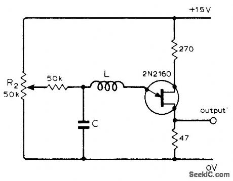
Uses unijunction transistor as negative resistance in simple RLC circuit, Maximum output with good waveform is about 200 mV. Exact frequency depends on values used for L and C.-R. P. Hart. Simple SineWave Oscillator, Wireless World. July 1976. p 34. (View)
View full Circuit Diagram | Comments | Reading(1314)
INITIALIZING_CMOS_STORAGE
Published:2009/7/5 20:42:00 Author:May
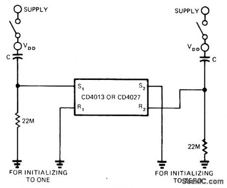
Simple RC circuit initializes all storage elements (flip-flops, registers, and counters) of CMOS system to all 1s (switch at left) or all 0s (switch at right) when power supply is turned on. For most CMOS storage elements, 30 pF for C ensures setting or resetting when power is applied by closing switch. If power supply is turned on while supply line is directly connected,C should be 1000 to 1500 pF Article also shows how to get set or reset function after initialization by uslng pairof CD4016A or CD4066A transmission gates,-o,Bismarck,A Simple Method for lnitiaizing CMOS Storage Elements,EDN Magazine, Feb.20,1974.p83 (View)
View full Circuit Diagram | Comments | Reading(843)
110_MHz_ON_SEVENTH_OVERTONE
Published:2009/7/5 20:41:00 Author:May
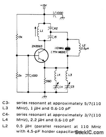
Requires only one doubler for use in 220-MHz amateur band Series-resonant traps are at frequencies of undesired lower modes.-H. Olson、 Frequency Synthesizer for 220 MHz,Ham Radio,Dec .1974,p 8-14. (View)
View full Circuit Diagram | Comments | Reading(497)
1000_Hz_WITH_ONE_CHIP
Published:2009/7/5 20:39:00 Author:May
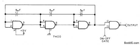
Quad NAND gate gives sawtooth output waveform at 800 to 1000 Hz for driving other TTL circuits.-Circuits. 73 Magazine. June 1977.p 49 (View)
View full Circuit Diagram | Comments | Reading(510)
DOUBLING_100_MHz
Published:2009/7/5 20:35:00 Author:May
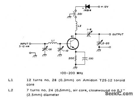
Recommended for use with VHF/UHF converters having inputs of 90 to120 MHz .Diode in series with power suρply prevents damage if the polarity is reversed.-J.Reiset, VHF/UHF Techniques,Ham Radio, March 1976,p 44-48. (View)
View full Circuit Diagram | Comments | Reading(470)
12_V_PROGRAMMER_FOR_PROM
Published:2009/7/5 20:31:00 Author:May
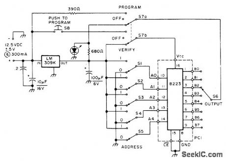
Circuit includes regulator for operation from 12-V auto storage battery. Developed to use 8223 32-word by 8-bit memory as CW identifier. All outputs of memory are initially at logic 0, so only logic 1s need to be programmed. After programming a 1, LED comes on to confirm it when S7 is switched to VERIFY. Do not hold S8 down longer than 1 s.-G. W. Kufchak, The PROM Zapper, 73 Magazine, Sept. 1976, p 112. (View)
View full Circuit Diagram | Comments | Reading(670)
HIGH_SPEED_FIFO
Published:2009/7/5 20:27:00 Author:May

Design is based on Motorola MC10143 register file, with each IC holding 8 words by 2 bits, Circuitincludes write and read enable inputs for cascading two register file packages to memory depth of 16 words. Full master-slave flip-flop operation allows simultaneous read and write. Reset is applied initially to drive both address counters to empty state.To enter data, write clock input is enabled with negative-going pulse. Write addressing is controlled by MC10178 binary counter. Used for stack registers of computing systems when register outputs are read sequentlally in sameorder that data wad entered(first-in first-out).-B.Blood, A High Speed FIFO Memory Usingthe MECL MC10143 Register Fil, Motorola,Phoenix,AZ,1974,AN-730,p 5. (View)
View full Circuit Diagram | Comments | Reading(1549)
| Pages:275/471 At 20261262263264265266267268269270271272273274275276277278279280Under 20 |
Circuit Categories
power supply circuit
Amplifier Circuit
Basic Circuit
LED and Light Circuit
Sensor Circuit
Signal Processing
Electrical Equipment Circuit
Control Circuit
Remote Control Circuit
A/D-D/A Converter Circuit
Audio Circuit
Measuring and Test Circuit
Communication Circuit
Computer-Related Circuit
555 Circuit
Automotive Circuit
Repairing Circuit