
Basic Circuit
Index 268
DPSK_ON_DSBSC
Published:2009/7/6 1:12:00 Author:May
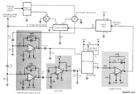
Differential phase-shift keyed double-sideband suppressed-carrier signal is demodulated by reinsertion of missing carrier, using synchronous or coherent detection. Receiver input signal is multiplexed by locally generated carrier, accurately controlled in frequency and phase. This is followed by low-pass filtering. Demodulation at output is by frequency/phase controlled loop that automatically locks local oscillator in frequency and phase to received vestige of carrier. This extracts phase information from modulated signal. Power divider is BF Associates H22, quad hybrid is Merrimac Research QHT-2, 0°and 90° phase detectors are Relcom M6A, and multiplier is Analog Devices 4281. Article covers theory and operation of circuit in detail.-R. Hennick, Demodulate DPSK Signals Coherently Using a Costas Phase-Lock Loop, EDN Magazine, July 1, 1972, p 44-47. (View)
View full Circuit Diagram | Comments | Reading(1718)
PHASE_COMPARATOR
Published:2009/7/6 1:09:00 Author:May

Signetic balanced moudulator-demodulator transistor array is connected as phase detector in which output contains term related to cosine of phase angle, Equal-frequency input signals are multiplied together by IC to produce sum and difference frequencies. Difference component becomes DC, while undesired sum component is related to phase angle, with cosine becoming 0 at 90° and having maximum positive or negaitive value at 0° and 80° respectively. Balanced modulator provides excellent conversion linearity along with conversion gain.-“Signetics Analog Date Manual,” Signetics, Sunnyvale, CA, 1977, p, 757-758. (View)
View full Circuit Diagram | Comments | Reading(4438)
0_360°PHASE_SHIFTER
Published:2009/7/6 1:09:00 Author:May

Each J202 JFET stage provides up to 180° phase shift under control of 1-megohm pot. Ganged pots give full range of control. JFETs specified are ideal for circuit be-cause they do not load phase-shift networks.- FET Databook, National Semiconductor, Santa Clara, CA, 1977, p 6-26-6-36. (View)
View full Circuit Diagram | Comments | Reading(1001)
PHOTOMULTIPLIER_OUTPUT_GATING_CIRCUIT
Published:2009/7/6 1:08:00 Author:May
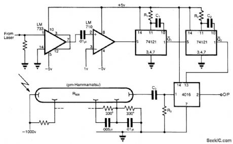
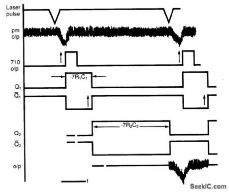
Circuit NotesThe application involves observing the light pulse emerging from a thick specimen after transillumination by a laser pulse. Pulses derived from the laser source are amplified using a Video Amplifier LM733. The reference level is set to 1 V in the comparator LM 710, to provide the necessary trigger pulses for the monostable multivibrator 74121.The laser pulses have a repetition frequency of 500 Hz and suitable values are as below:
R1= 33 k ohm, C1 = 22 pFR2 = 33 k ohm, C2 = 68 nF
The pulse width for each monostable is approximately given by tw=0.7 RC. R3 and C3 is a high pass filter. The method therefore permits the use of low cost components having moderate response times for extracting the pulse of interest. (View)
View full Circuit Diagram | Comments | Reading(1838)
VOLTAGE_CONTROLLED_PHASE_SHIFTER
Published:2009/7/6 1:06:00 Author:May
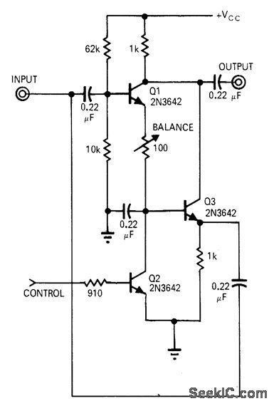
Circuit shifts carrier 180° by sensing polarity of modulating voltage. Operating range is 5 kHz to 10 MHz. Circuit can also be used to convert unipolar pulses to alternate bipolar pulses or vice versa when synchronized square wave is sup-plied to control input. With 0 V at base of Q2, Q3 will amplify RF voltage applied to input, without phase shift. To actuate switch and provide 180° phase shift, positive voltage is applied to base of Q2 so it saturates and cuts off, allowing Q1 to conduct. Output then appears across load with phase reversed.-A. H. Hargrove, Simple Circuits Control Phase-Shift, EDN Magazine, Jan. 1, 1971, p 39. (View)
View full Circuit Diagram | Comments | Reading(1868)
Radio Cassette Player and Air Conditioning Principle Diagram of Liberation CA6440 Series Light Bus
Published:2011/7/20 0:26:00 Author:Michel | Keyword: Liberation, Light Bus, Radio Cassette Player, Air Conditioning, Principle Diagram

Picture:Radio Cassette Player and Air Conditioning Principle Diagram of CA6440 Series Light Bus
75-instrument light,77-antenna of radio cassette player,78-radio cassette player ,79 and 80-loudspeaker,81-electronic clock,82-warm wind motor relay,83-heater motor,84-warm wind switch ,85-variable speed resistance ,86 and 87-micro switch ,88-drum wind (air conditioning) motor relay . (View)
View full Circuit Diagram | Comments | Reading(1081)
FULL_WAVE_FEEDBACK
Published:2009/7/6 1:06:00 Author:May
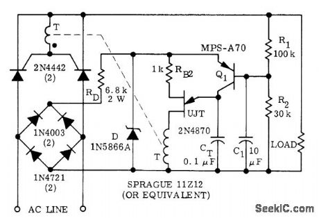
Used when average load voltage is desired feedback variable for full-wave phase control of load power. Circuit requires use of pulse transformer T.-D. A. Zinder, Unijunction Trigger Circuits for Gated Thyristors, , Motorola, Phoenix, AZ, 1974, AN-413, p 4. (View)
View full Circuit Diagram | Comments | Reading(749)
AF_PLL
Published:2009/7/6 1:04:00 Author:May

Addition of components to conventional two-transistor MVBR gives simple phase-locked loop. Tr1 and diode form logic gate that conducts during alternate half-cycles of input and VCO waveforms respectively. Output of this phase detector, when filtered, is most negative when waveforms are in phase, and most positive when they are out of phase. Once phase lock has been established, it is maintained by VCO over range of 100 to 3000 Hz.-J. B. Cole, Simple Phase-Locked Loop, Wireless World, June 1977, p 56. (View)
View full Circuit Diagram | Comments | Reading(2411)
WIDE_CAPTURE_RANGE_FOR_PLL
Published:2009/7/6 1:03:00 Author:May
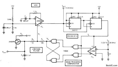
Fast wide-band phase-locked loop uses one Am686latch-ing comparator as voltage-controlled oscillator, while other is coupled with TTL latch to produce edge-triggered comparator. VCO and comparator combined with low-pass filter R1-R2-C2 form PLL When locking fails, UJT causes VOUT to scan, repetitively sweeping all frequencies in VCO range until lock is restored,Capture and locking ranges are both equal at ±60% for 5 MHz input.-M. C. Hahn, PLL’s Capture Range Equals Its Locking Range, EDN Magazine, Sept. 20, 1977, p 117 and 119-120. (View)
View full Circuit Diagram | Comments | Reading(1409)
Cigar Lighter,Wiping and Washing Circuit Principle Diagram of Liberation CA6440 Series Light Buses
Published:2011/7/20 0:56:00 Author:Michel | Keyword: Liberation, Light Buses, Cigar Lighter, Wiping, Washing, Principle Diagram

Picture:Cigar Lighter,Wiping and Washing of CA6440 Series Light Buses
89-drum wind (air conditioning) motor ,90-temperature control switch ,91-low voltage switch ,92-high voltage cutout switch,93-compressor electromagnetic clutch ,94-cigar lighter,95-washer motor,96-washing motor switch ,97-wiper,98-wiper switch,100-air conditioning floodlight ,Fl-Fl4一fuse.
(View)
View full Circuit Diagram | Comments | Reading(883)
8_bit_straight_binary_D_A_converter
Published:2009/7/23 21:41:00 Author:Jessie
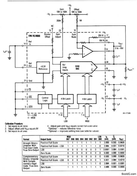
This circuit uses a DAC-4888 and a few external components to form a stand-alone, 0- to + 10-V, D/A converter with both gain and offset adjustments for calibration. (View)
View full Circuit Diagram | Comments | Reading(630)
0_90°_SHIFTER
Published:2009/7/6 1:02:00 Author:May
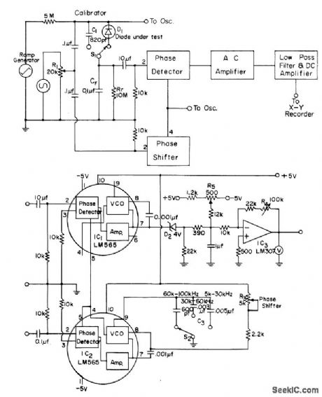
Used in automatic plotter for measuring capacitance-voltage characteristics of Schottky barrier solar cells. Diode under test is connected as shown in block diagram. Phase of square-wave output from IC, can be shifted continuously from 0 to 90° by adjusting R3. Article gives ramp circuit and design equations.-J. T. Lue, An Automatic C-V Plotter and Junction Parameter Measurements of MIS Schottky Barrier Diodes, IEEE Journal of Solid-State Circuits, Aug. 1978, p 510-514. (View)
View full Circuit Diagram | Comments | Reading(645)
PHASE_LOCKED_100_kHz_REFERENCE
Published:2009/7/6 1:01:00 Author:May

Uses 4-MHz crystal in oscillator, with voltage-variable capacitor VVC in parallel with fixed and variable capacitors for setting frequency precisely. Varicap or silicon diode can also be used for VVC. Control voltage for WC is developed by Motorola MC4044P phase-frequency detector and associated MPSA20 amplifier and filter. 7473 and 7490 ICs divide 4-MHz signal by 4 and then by 10 to give 100 kHz. Main output can be further divided with additional 7490s, down to 60 Hz for driving electric clock if desired. Adjust C3 and R1 for symmetrical square wave at pin 1 of MC4044P, with clean leading and trailing edges. Typical values are 68 pF for C3 and 300K for R1, but values will depend on transistors used. Transistor types are not critical. Gates U2B and U2C with Q3 form lock indicator circuit that turns on LED when 4-MHz oscillator is phase-locked to output of external high-stability 100-kHz frequency standard. U1 and U2 are SN7400.-C. A. Harvey, How to Improve the Accuracy of Your Frequency Counter, Ham Radio, Oct. 1977, p 26-28. (View)
View full Circuit Diagram | Comments | Reading(981)
SINE_WAVE_WIEN
Published:2009/7/6 0:58:00 Author:May
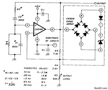
Uses CA3140 opamp and diode array to generate low-distortion sine waves. Table gives values recommended for R and C to obtain frequencies from 50 Hz to 30 kHz. Use of zener diode clamp for amplitude control gives fast AGC.-W. Jung, An IC Op Amp Update, Ham Radio, March 1978, p 62-69. (View)
View full Circuit Diagram | Comments | Reading(1101)
Microprocessor_supervisor_with_internal_backup_battery
Published:2009/7/23 21:41:00 Author:Jessie
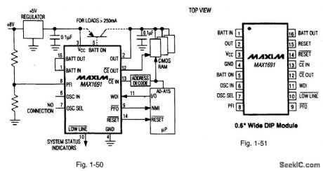
Figures 1-50 and 1-51 show a typical application circuit and pin configuration, respectively, for the MAX1691. The IC switches over to an internal backup battery to provide write protection and a watchdog function. The internal 3-V 125-mAh lithium battery connects to the supervisory circuit through external pin strapping (to minimize battery drain during shipping.) The IC is shipped in special nonconductive material. Storing the IC in conductive foam will discharge the internal battery. The power-OK/reset time delay is 200 ms, and standby current is 1μA, with a typical 35-μA operating current. On-board gating of the chip-enable signals has a maximum delay of 10 ns. MAXIM NEW RELEASES DATA BOOK, 1995, P. 5-7. (View)
View full Circuit Diagram | Comments | Reading(777)
4_46_MHz_TUNABLE
Published:2009/7/6 0:57:00 Author:May

Emitter-follower buffer stage for isolation has low-pass filter for reducing harmonic output and giving better sine-wave output. Oscillator coil should be in shield at least twice coil diameter.-An Accessory VFO-the Easy Way, 73 Magazine, Aug. 1975, p 103 and 106-108. (View)
View full Circuit Diagram | Comments | Reading(843)
15_65_MHz_THIRD_OVERTONE
Published:2009/7/6 0:56:00 Author:May

Crystal starting is reliable, and power dissipation of crystal is well below allowable maximum. Q1 is 2N918, 2N3564, 2N5770, BF180, or BF200. L1 resonates at crystal frequency with 22 pF (1μH for 15-30 MHz or 0.5μH for 30-65 MHz). Stability is as good as that of fundamental-frequency oscillator. Set L1 roughly to frequency with no supply voltage by shorting crystal and dipping L1 with grid-dip oscillator. Now apply power and tune L1 close to marked crystal frequency while monitoring output frequency. Remove short and trim to frequency with 3-30 pF trimmer.-R. Harrison, Survey of Crystal Oscillators, Ham Radio, March 1976, p 10-22. (View)
View full Circuit Diagram | Comments | Reading(2061)
283_MHz_THIRD_OVERTONE_TTL
Published:2009/7/6 0:55:00 Author:May

Third-over-tone crystal oscillator uses 74S00 Schottky TTL quad NAND gates acting as oscillator and output buffer to increase output amplitude. Output swing is from about 0.4 to 3.5 V P-P, as required for TTL. No inductors are required.-C. Hall, Overtone Crystal Oscillators Without Inductors, Ham Radio, April 1978, p 50-51. (View)
View full Circuit Diagram | Comments | Reading(1743)
18_60_MHz_THIRD_OVERTONE
Published:2009/7/6 0:55:00 Author:May

International Crystal OF-1 oscillator for third-overtone crystals requires no inductors. Crystal operates near series resonance, making capacitor unnecessary in series with crystal. With 28.3-MHz third-overtone crystal, circuit delivers 28.3 MHz when C1 is 100 pF and C2 is 18 pF. Using larger values given in table produces oscillation at fundamental of 9.43 MHz.-C. Hall, Overtone Crystal Oscillators Without Inductors, Ham Radio, April 1978, p 50-51. (View)
View full Circuit Diagram | Comments | Reading(2223)
1850_Hz_DIGITAL_IC
Published:2009/7/6 0:46:00 Author:May

Two sections of RS7404 hex inverter are connected as astable MVBR operating at frequency determined by values used for C1 and C2. Output drives loudspeaker as shown to produce audible tones or can be connected to flash LEDs. D1 reduces battery voltage to 5 V required by 1C. Developed for classroom demonstrations. Circuit produces nearly square waves with amplitude of about 3 V and pulse width of about μ100 pos if used as squarewave generator.-F. M. Mims, Integrated Circuit Projects, Vol. 6. Radio Shack. Fort Worth. TX, 1977, p 64-69. (View)
View full Circuit Diagram | Comments | Reading(756)
| Pages:268/471 At 20261262263264265266267268269270271272273274275276277278279280Under 20 |
Circuit Categories
power supply circuit
Amplifier Circuit
Basic Circuit
LED and Light Circuit
Sensor Circuit
Signal Processing
Electrical Equipment Circuit
Control Circuit
Remote Control Circuit
A/D-D/A Converter Circuit
Audio Circuit
Measuring and Test Circuit
Communication Circuit
Computer-Related Circuit
555 Circuit
Automotive Circuit
Repairing Circuit