
Basic Circuit
Index 262
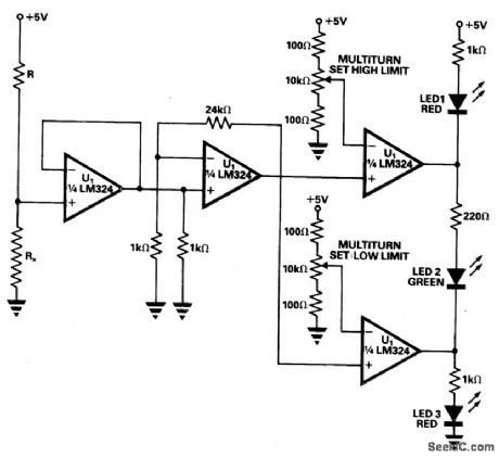
SINGLE_CHIP_CHECKS_RESISTANCE
Published:2009/7/6 3:44:00 Author:May
Circuit Notes
A simple tester can be used for routine checks for resistance on production lines of relays, coils, or similar components where frequent changes in resistance to be tested are not required. The tester is built around a single quad op amp chip, the LM324. R, which is chosen to be around 80 times the resistance to be checked, and the 5 V supply form the current source. The first op amp buffers the voltage generated across the resistance under test, Rx. The second op amp amplifies this voltage. The third and fourth op amps compare the amplified voltage with high and low limits. The high and low limits are segt on multiturn presets with high and low limit resistors connected in place of Rx. LED 1 (red) lights when the resistance is high. LED 2 (greep) shows that the resistance is within limits. LED 3 (red) indicates that the resistance is low. (View)
View full Circuit Diagram | Comments | Reading(637)
SINE_WAVE_SHAPER_
Published:2009/7/6 3:42:00 Author:May

Uses CA3140 opamp as voltage follower, acting with diodes from CA3019 array to convert triangle output of function generator or other source to sine wave having total harmonic distortion typically less than 2%.- Circuit Ideas for RCA Linear ICs, RCA Solid State Division, Somelville, NJ, 1977, p 5. (View)
View full Circuit Diagram | Comments | Reading(2005)
COURTESY_LIGHT_EXTENDER
Published:2009/7/6 3:42:00 Author:May
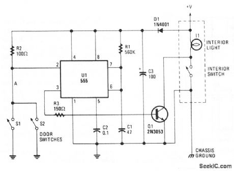
The circuit keeps the courtesy light on for 30 seconds after you close the door. The lead from the door switch is removed and connected to the 555 circuit. The 555 is arranged in a monostable mode, and is triggered by the door switches. The output drives Q1, which is connected across the interior light switch.The interior light is turned on for 30 seconds after the door is opened. If the door(s) are held open for longer than 30 seconds, it will not reset until after the doors are closed. In that case, the lights go out immediately. (View)
View full Circuit Diagram | Comments | Reading(1438)
ELECTRONIC_CAR_HORN
Published:2009/7/6 3:41:00 Author:May
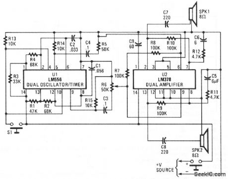
An LM556 dual oscillator/timer, U1, configured as a two-tone oscillator drives U2,a dual 4-watt amplifier. One of the oscillators, pins 1 to 6, contained in U1 produces the upper frequency signal of about 200 Hz, while the second oscillator, pins 8 to 13, provides the lower frequency signal of about 140 Hz. Increase or decrease the frequencies by changing the values of C2 and C3. U1's outputs,pins 9 and 5, are connected to separate potentiometers to provide control over volume and balance. Each half of U2 produces 4 W of audio that is delivered to two 8-Ω loudspeakers via capacitors C7 and C8. (View)
View full Circuit Diagram | Comments | Reading(1373)
BACK_UP_BEEPER
Published:2009/7/6 3:39:00 Author:May
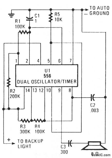
Put the car in reverse and the circuit provides a loud, audible beep at the rate of about one per second (1 Hz). Half of U1, a 556 dual oscillator/timer, is used as a slow-pulse oscillator with a rate of about 1 Hz. Components R2, R1, and C1 form the long time constant. You can calculate on time by t=.7 (R1 + R2) C1 or 1.15 seconds. The off time is shorter than the on time, at.77 second. Enabling pin 4 (reset) is held high to keep the oscillator freerunning when voltage is applied to pin 14. The output at pin 5 is coupled to pin 10 of U1 enabling oscillator 2. Oscillator 2 of U1 produces an audio output of about 1 kHz, as determined by C2, R3, and R4. Pin 10 (reset) of oscillator 2 is connected to the pin 5 output of oscillator 1. So when pin 5 becomes positive, the oscillator beeps a short pulsed tone of 1 kHz. (View)
View full Circuit Diagram | Comments | Reading(712)
AUTOMATIC_HEADLIGHT_DELAY
Published:2009/7/6 3:36:00 Author:May
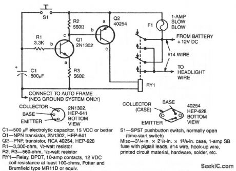
When the driver depresses pushbutton switch S1, timing capacitor C1 charges to 12 V and turns on transistor Q1, which drives power transistor Q2 into conduction. This, in turn, energizes the relay which has its contacts connected in parallel with the headlight switch. The relay will stay energized until C1 discharges to the Q1 turn-off level. The lights-on period is determined by the value of C1, R1, and the charac-teristics of transistor Q1. With values chosen on the schematic, about 60 light-on seconds are provided.
(View)
View full Circuit Diagram | Comments | Reading(702)
AUTOMOBILE_VOLTAGE_REGULATOR
Published:2009/7/6 3:32:00 Author:May
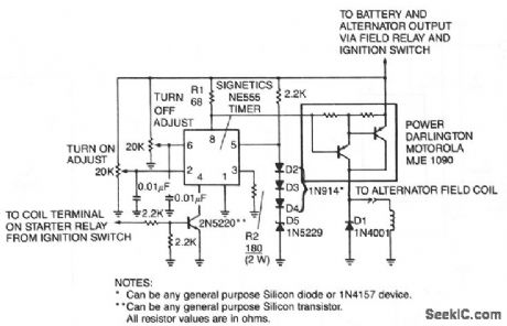
A monolithic 555-type timer is the heart of this simple automobile voltage regulator. When the timer is off so that its output at pln 3 is low,the power Darlington transistor par is off.If battery voltage becomestoo low,less than 14.4 V in this case,the timer turns on and the Darlington par conducts. (View)
View full Circuit Diagram | Comments | Reading(1845)
TACHOMETER_WITH_SET_POINT
Published:2009/7/6 3:28:00 Author:May
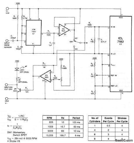
View full Circuit Diagram | Comments | Reading(1206)
DIVIDE_BY_5_WITH_TWO_GATES_AND_3_BITS
Published:2009/7/6 3:28:00 Author:May
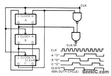
Arrangement shown for dlviding clock inputfrequency by 5 requires onlytwo gates from 846 IC and 3 bits of 852 JK flip-flop storage to glve square-wave output pulses having 50% duty cycle.-C,L,Maginnlss, Another Reader Respondsto Odd Modulo Dlvider,EDN Magazine,Oct,15,1972,p 57. (View)
View full Circuit Diagram | Comments | Reading(736)
SYMMETRICAL_DIVIDE_BY_5_CLOCK
Published:2009/7/6 3:27:00 Author:May
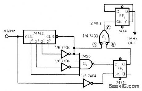
Uses 74163 counter to generate two phases of 1-MHz clock pulse with 50% duty cycle from 5-MHz system reference. One phase is decode of binary 4 from counter, while other is decode of 1 clocked at midbit time. Both phases are recombined in gate G1 to give 2-MHz clock that toggles FF2 to generate desired 1-MHz output.-L. A.Mann, Divider Circuit Maintains Pulse Symmetry, EDN Magazine, July 1, 1972, p 54-55. (View)
View full Circuit Diagram | Comments | Reading(922)
10_MHz_FRONT_END
Published:2009/7/6 3:25:00 Author:May
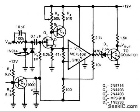
Front-end design for battery-operated 5-MHz counter consists of FET and bipolar buffer followed by Schmitt trigger made from MC75108 dual line receiver. Circuit operates linearly upto 10 MHz with 25-mV input signal. Requires swings from logic 0 (0 V) to logic 1(about 10 V), for which suitable counter circuit is given in article. Accepts any input waveform shape and level.-D. Aldridge, CMOS Counter Circuitry Slashes Battery Power Requirements, EDN Magazine, Oct. 20, 1974, p 65-71. (View)
View full Circuit Diagram | Comments | Reading(743)
TR_CIRCUIT
Published:2009/7/6 3:23:00 Author:May
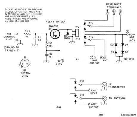
Circuit Notes
C1 and C2 are disc ceramic. R1 and R2 are 1/4 or 1/2 W carbon composition resistors. K1 is a 12 V DPDT DIP relay. Illustration A shows how to connect the relay contacts for use with a separate transmitter-receiver combination. The circuit at B is for amplifier use with a transceiver. (View)
View full Circuit Diagram | Comments | Reading(684)
SOUARE_WAVE_DIVIDER
Published:2009/7/6 3:22:00 Author:May
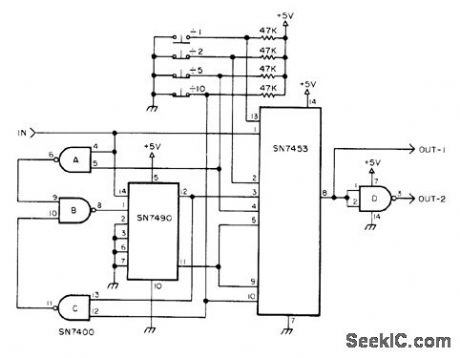
Divides input square wave by 1, 2, 5, or 10 depending on which switch is open. Signal at OUT-1 is inverted with respect to input, and OUT-2 is noninverted.-Circuits, 73 Magazine, June 1977, p 49. (View)
View full Circuit Diagram | Comments | Reading(775)
Basic_8080_8224_8228_interface_for_A_D_converter
Published:2009/7/23 20:43:00 Author:Jessie
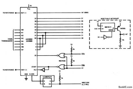
This circuit shows a minimum-component interface for the ADC0808/ 0809, where the EOC is tied directly to the 8080 interrupt input. If an INS8228 is used and the INTA pin is tied through a 1-kΩ resistor, the interrupt will cause a restart, RST, to be executed. This causes a jump to a restart vector, and execution of the interrupt. If a very simple multi-interrupt system is desired, a wired-OR configuration using resetable latches (as shown in dashed lines) can be used. Figures 6-21 and 6-22 show the I/O port-address structures. (View)
View full Circuit Diagram | Comments | Reading(1118)
DIVIDE_BY_5
Published:2009/7/6 3:20:00 Author:May

Requires only two digital chip types, Input clock is alternately inverted and noninverted for clocking divide-by-3 counter, to give effect of dividing by 21/2 which toggles A3 to give symmetrical divide-by-5 output with 50% duty cycle for pulses. Article gives timing diagram and traces operation of circuit.-C. W.Hardy, Reader Responds to Odd Modulo Divider in July 1st EDN, EDN Magazine, Oct. 1, 1972, p 50. (View)
View full Circuit Diagram | Comments | Reading(2245)
3_TO_29_ODD_MODULO
Published:2009/7/6 3:19:00 Author:May
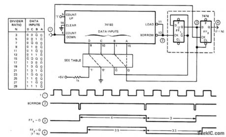
Basic dlvider using 74193 4-bit up/down counter and single 7474 dual D flip-flop provides any odd number of dlvider ratios from 3 to 29 by changing feedback connections as shown in table, all with symmetrical output waveforms. Based on writing any odd number N as N = M + (M + 1), where M is integer. Circuit forces counter to divide altemately by M and M + 1. Connection shown is for divide-by-7.-V. R. Godbole, Simplify Design of Fixed Odd-Modulo Dividers, EDN Magazine, June 5, 1975, p 77-78.
(View)
View full Circuit Diagram | Comments | Reading(2238)
10_Hz_TO_2_MHz
Published:2009/7/6 3:19:00 Author:May
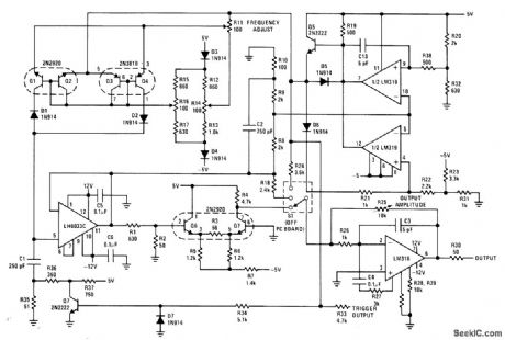
Triangle wave is generated by switching current-source transistors to charge and discharge timing capacitor. Precision dual comparator sets peak-to-peak amplitude. Sine converter requires close amplitude control to give low-distortion output from triangle input.Square-wave output is obtained at emitter of Q5, for driving current switches Q1-Q4 and LM318 output amplifier. Scaling permits adjusting all three waveforms to ±10 V. Waveforms are symmetrical up to 1 MHz, and output is usable to about 2 MHz.-R. C. Dobkin, Wide Range Function Generator, National Semiconductor, Santa Clara, CA, 1974, AN-115. (View)
View full Circuit Diagram | Comments | Reading(0)
DIVIDE_BY_15
Published:2009/7/6 3:17:00 Author:May
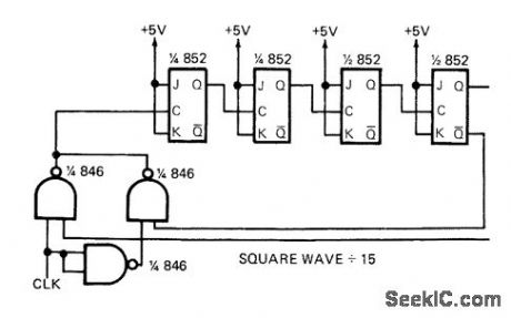
Input clock is altemately inverted and noninverted by gates operating in coniunction with 4 bits of storage using 852 JK flip-flops, to give square-wave output at 1/15 of clock frequency.-C. W. Hardy, Reader Responds to Odd Modulo Divider in July 1st EDN, EDN Magazine, Oct, 1, 1972, p 50. (View)
View full Circuit Diagram | Comments | Reading(668)
Parallel_data_acquisition_with_sample_hold
Published:2009/7/23 20:38:00 Author:Jessie

This circuit uses ADC0808/0809 ICs and LF398 sample/hold ICs to form an 8-channel parallel data-acquisition system. Sample/hold is accessed through an MM74C42 which pulses an MM74C221, generating a sample pulse. After each sample/hold has sampled the signal, the appropriate channel information is processed by the ADC (as described in Fig.6-13). (View)
View full Circuit Diagram | Comments | Reading(1718)
RELAY_DRIVER_PROVIDES_DELAΥ_AND_CONTROLS_CLOSURE_TIME
Published:2009/7/6 3:17:00 Author:May

Circuit NotesThe relay operates a certain time, td, after power is applied to it, and then it operatesfor a leng付1 of time, tCThe SCR fires when the voltage on C1 reaches VA.This operatesthe relay, which stays activated until the current charging C2 drops below the dropoutcurrent. 10 keep the relay In its activated position indefinitely(tc=∞), ellmlnate C2and choose R2 just large enough to keep the relay coil current within its related limits, Typical component values for td=30 seconds and tc=2 seconds are∶ R1=1.5megohms, R2 = 10 k ohms, R3 =3 k ohms, C1=47μF, and C2 =100μF. TheSCR is a 2N1877 and the relay is a Potter Brumfield PW-5374. A value of 12 Vdc ISassumed for Vcc. (View)
View full Circuit Diagram | Comments | Reading(697)
| Pages:262/471 At 20261262263264265266267268269270271272273274275276277278279280Under 20 |
Circuit Categories
power supply circuit
Amplifier Circuit
Basic Circuit
LED and Light Circuit
Sensor Circuit
Signal Processing
Electrical Equipment Circuit
Control Circuit
Remote Control Circuit
A/D-D/A Converter Circuit
Audio Circuit
Measuring and Test Circuit
Communication Circuit
Computer-Related Circuit
555 Circuit
Automotive Circuit
Repairing Circuit