
Basic Circuit
Index 273
UART_INTERFACE
Published:2009/7/5 22:19:00 Author:May

Uses TMS-6011 UART to convert parallel data into serial data and back again for Altair 8800 microprocessor. UART mates directlyto computer bus, because all outputs from UART are three-state buffers with separate enable lines provided for status bits and 8 bits of parallel output. Pin 22 is high when UART can accept another character for conversion. Pin 18 must be pulsed low to reset pin 19 so it can signal receipt of another character.Connections to pins 35-39 depend on I/0 devices used, as covered in article.-W. T. Walters, Build a Universal I/O Board, Kilobaud, Oct. 1977, p 102-108. (View)
View full Circuit Diagram | Comments | Reading(2407)
THREE_PHASE_SWITCH_FOR_INDUCTIVE_LOAD
Published:2009/7/5 22:18:00 Author:May
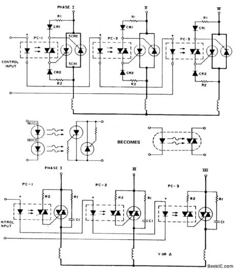
The following are three-phase switches for low voltage. Higher currents can be ob-tained by using inverse parallel SCRs which would be triggered as shown. To simplify the following schematics and facilitate easy understanding of the principles involved, the following schematic substitution is used (Note the triac driver is of limited use at 3 φ voltage levels). (View)
View full Circuit Diagram | Comments | Reading(563)
1_9_kHz_PLL
Published:2009/7/5 22:15:00 Author:May
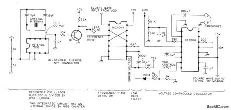
Simple experimental phase locked loop circuit synthesizesfrequencies in audio range, for easy monitoring with headphones.Article gives theory of operation and setup procedure.-.G.R.Allen ,Synthesize Yourself,73Magazine,Oct.1977,p 182-188. (View)
View full Circuit Diagram | Comments | Reading(1964)
AUTORANGING_FOR_DATA_ACQUISITION
Published:2009/7/5 22:14:00 Author:May
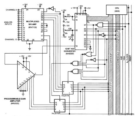
Circuit accepts up to 16 channels of analog information and provides full-scale input ranges from ± 78 mV to ± 10 V when used with 6800 CPU. Resolution is 0.01%. MN7130 multiplexed sample-and-hold amplifier includes eight full differential multiplexers for 16 channels and instrumentation opamp. MN2020 programmablegain amplifier provides choice of eight gains ranging from 1 to 128 in binary progression. Autoranging operation of data acquisition system allows channel-sampling plans that depend on random events. With known input signallevels, required gain information can be stored in microprocessor memory for use in place of autoranging,-R. Duris and J. Munn, PGA's Give Your DAS Designs Autoranging, Wide Dynamic Range, EDN Magazine, Sept. 5, 1978, p 137-141. (View)
View full Circuit Diagram | Comments | Reading(596)
PASSIVE_BRIDGED,DIFFERENTIATOR_TUNABLE_NOTCH_FILTER
Published:2009/7/5 22:14:00 Author:May

View full Circuit Diagram | Comments | Reading(1136)
WIEN_BRIDGE_NOTCH_FILTER
Published:2009/7/5 22:12:00 Author:May

View full Circuit Diagram | Comments | Reading(856)
ACTIVE_BAND_REJECT_FILTER
Published:2009/7/5 22:12:00 Author:May

A filter with a band-reject characteristic is frequently referred to as a notch filter.A typical circuit using a μA741 is the unity-gain configuration for this type of active filter shown. The filter response curve shown is a second-order band-reject filter with a notch frequency of 3 kHz. The resulting Q of this filter is about 23, with a notch depth of -31 dB. Although three passive T networks are used in this application, the operational amplifier has become a sharply tuned low-frequency filter without the use of inductors or large-value capacitors. (View)
View full Circuit Diagram | Comments | Reading(4653)
WIEN_BRIDGE_AF_RF
Published:2009/7/5 22:11:00 Author:May
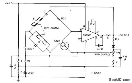
Single JFET in basic Wien-bridge circuit drives Texas Instruments linear opamp serving as output stage. Feedback path from output of ICto base of JFET stabilizes output and provides temperature compensation. Dual pot in bridge circuit serves for frequency control, Circuit performs well as either AF or RF oscillatordepending on values used for R and C.-E. M. Noll, FET Prinqiples, Experiments, and Projects, Howard W. Sams, Indianapolis, IN, 2nd Ed., 1975, p 213-214. (View)
View full Circuit Diagram | Comments | Reading(501)
AUDIO_NOTCH_FILTER
Published:2009/7/5 22:10:00 Author:May


With the circuit shown here the response at one octave off tune is within 10% of the far out response: notch sharpness may be increased or reduced by reducing or increasing respectively the 68 K ohm resistor. Linearity tracking of R8 and R9 has no effect on notch depth. The signals at HP and LP are always in antiphase, notch will always be very deep at the tuned frequency, despite tolerance variations in R6-9 and C2, C3. (View)
View full Circuit Diagram | Comments | Reading(1026)
TUNABLE_AUDIO_NOTCH_FILTER_CIRCUIT
Published:2009/7/5 22:09:00 Author:May

The circuit requires only one dual-ganged potentiometer to tune over a wide range ; if necessary over the entire audio range in one sweep. The principle used is that of the Wien bridge, fed from anti-phase inputs. The output should be buffered as shown with a FET input op amp, particularly if a high value pot is used. An op amp with differential outputs (eg., MC1445) may be used in place of the driver ICS; R2 may be made trimmable to optimize the notch. (View)
View full Circuit Diagram | Comments | Reading(2180)
550_Hz_NOTCH_FILTER
Published:2009/7/5 22:08:00 Author:May

The circuit produces at least 60 dB of attenuation。f the notch frequency. (View)
View full Circuit Diagram | Comments | Reading(889)
1800_Hz_NOTCH_FILTER
Published:2009/7/5 22:07:00 Author:May

The circuit produces at least 60 dB of attenuation of the notch frequency. (View)
View full Circuit Diagram | Comments | Reading(713)
ADJUSTABLE_Q_NOTCH_FILTER
Published:2009/7/5 22:07:00 Author:May

In applications where the rejected signal might deviate slightly from the null on the notch network, it is advantageous to lower the Q of the network. This insures some rejection over a wider range of input frequencies. The figure shows a circuit where the Q may be varied from 0.3 to 50. A fraction of the output is fed back to R3 and C3 by a second voltage follower, and the notch Q is dependent on the amount of signal fed back. A second follower is necessary to drive the twin T from a low-resistance source so that the notch frequency and depth will not change with the potentiometer setting. (View)
View full Circuit Diagram | Comments | Reading(0)
QTT533 Reset Function Voltage Regulated Integrated Circuit
Published:2011/7/29 9:36:00 Author:Michel | Keyword: Reset Function, Voltage Regulated, Integrated Circuit

First,Functions Features
QTT533 integrated circuit contains reset circuit, + 5 V power supply voltage stabilizer and so on.
Second,Pins Functions and Data
QTT533 integrated circuit uses pin single in-line package and its pins functions and data are shown as table 1.
Tip: When QTT533 integrated circuit is damaged and it can be subsituted by 78LRO5 directly.
Table 1:QTT533 IC Pins Functions and Data (View)
View full Circuit Diagram | Comments | Reading(698)
11_16_MHz_IN_10_Hz_STEPS
Published:2009/7/5 22:04:00 Author:May
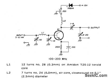
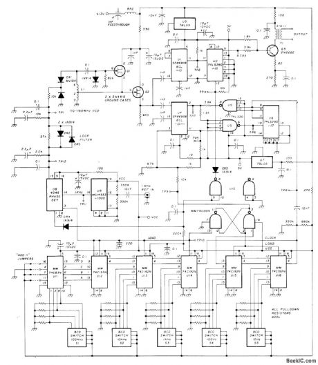
1.1-1.6 MHz IN 10-Hz STEPS-Data input re|quirement is parallel BCD with 10-V CM0S levels and five digits. Reference input is 1-MHz sine or square with at least 1 VP-P. VC0 covers 110-160 MHz in 1-kHz steps, operating in loop haying 1-kHz reference. VCO signal is divided by 100 to give final output in 10-Hz steps. L1 is 6 turns No. 22 on 3-mm form, tapped at 2 turns.RFC is 6 turns No. 28 on F754-1-06 ferrite bead.T1 is Mini-Circuits Lab T16-1 broadband RF transformer.-R. C. Petit, Frequency Synthesized Local-Oscillator System for the High-Frequency Amateur Bands, Ham Radio, Oct. 1978,p 60-65. (View)
View full Circuit Diagram | Comments | Reading(592)
Homemade wireless video doorbell circuit
Published:2011/7/26 2:14:00 Author:Christina | Keyword: Homemade, wireless, video doorbell
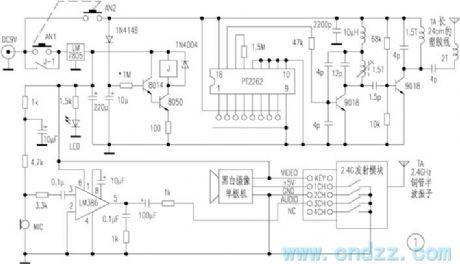
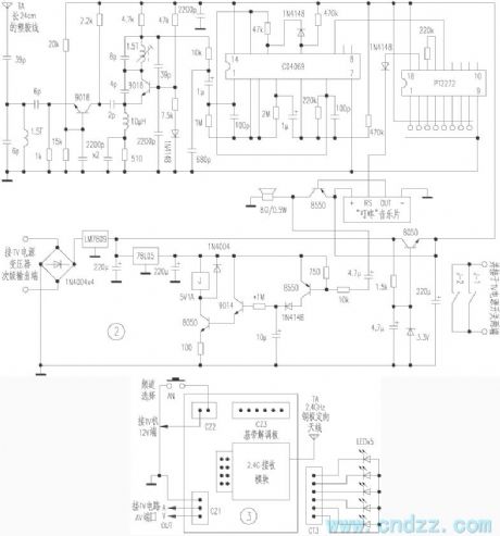
Figure 1 is the outdoor circuit, AN1 and AN2 are the buttons of the doorbell, when the guest presses the button of the doorbell, one channel of the power supply supplies the power to the coding launch circuit through the AN2, the coding launch circuit outputs the 315MHz coded signal, at the same time the power supply charges the 10μF timing capacitor through 1N4148. Another channel of the power supply supplies the power to the delay circuit through the AN1, the relay gets power to close, the contact point J-1 closes to protect itself. And the LM386 forms the voice pick-up circuit, the video camera and the 2.4GHz transmitter module all get power to work, the transmitter module outputs the high frequency signal which is modulated by the AV signal.
(View)
View full Circuit Diagram | Comments | Reading(2263)
001_ANALOG_MULTIPLIER
Published:2009/7/5 21:58:00 Author:May
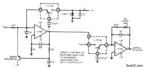
The F→V input frequency is locked to the U→F output because the LTC1043's clock is common to both sections. The F→V's reference is used as one input of the multiplier, while the U→F furnishes the other. To calibrate, short the X and Y inputs to 1.7320 V and trim for a 3-V output (View)
View full Circuit Diagram | Comments | Reading(612)
ANALOG_MULTIPLIER
Published:2009/7/5 21:57:00 Author:May

View full Circuit Diagram | Comments | Reading(1979)
10_Hz_WIEN_BRIDGE
Published:2009/7/5 21:54:00 Author:May
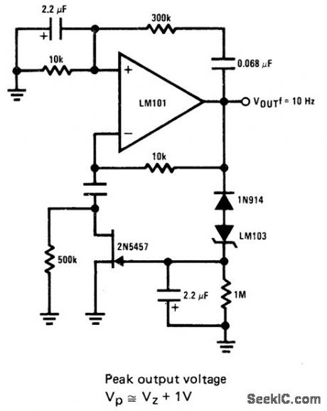
JFET serves as voltage-variable resistor in feedback loop of opamp. as required for producing low-distortion constant amplitude sine wave LM 103 zener providrs voltage for peak amplitude of sine wave this voltage is rectified and fed to gate of JFET to vary its channel resistance and loop gain of opamp.- FET Databook, National Semiconductor. Santa Clara. CA. 1977. p 6-26-6-63 (View)
View full Circuit Diagram | Comments | Reading(831)
Interfacing_D_A_converters_with_CMOS_and_ECL
Published:2009/7/23 21:59:00 Author:Jessie
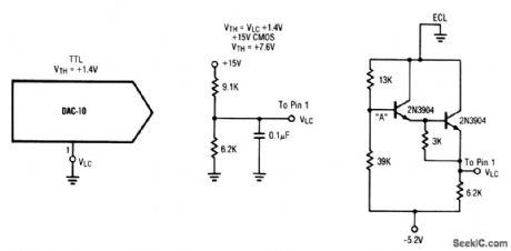
This circuit shows the interface circuits that are required to interface atypical TTL DAC (or similar IC) with ECL and CMOS digital devices. Note that HTL, PMOS, and NMOS devices can generally be interfaced with the CMOS circuit. (View)
View full Circuit Diagram | Comments | Reading(592)
| Pages:273/471 At 20261262263264265266267268269270271272273274275276277278279280Under 20 |
Circuit Categories
power supply circuit
Amplifier Circuit
Basic Circuit
LED and Light Circuit
Sensor Circuit
Signal Processing
Electrical Equipment Circuit
Control Circuit
Remote Control Circuit
A/D-D/A Converter Circuit
Audio Circuit
Measuring and Test Circuit
Communication Circuit
Computer-Related Circuit
555 Circuit
Automotive Circuit
Repairing Circuit