
Basic Circuit
Index 280
LOW_PASS_WITH_425_MHz_CUTOFF
Published:2009/7/3 4:12:00 Author:May

Designed for insertion in antenna coax of amateur radio station up to 1 kW, to cure TVI Problems.Provides 60-dB attenuation on channel 2. Filter uses mderived terminating half-sections at each end, with two constant-K midsections.End sections are tuned either to channel 2 (55 MHz) or channel3(61 MHz), Article covers construction and tune-up.-N. Johnson, High-Frequency Lowpass Filter, Ham Radio, March 1975, p 24-27. (View)
View full Circuit Diagram | Comments | Reading(626)
STEREO_DECODER_
Published:2009/7/3 4:11:00 Author:May
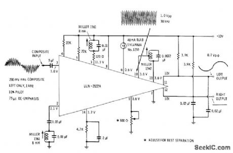
Single Sprague ULN-2122A IC is driven by composite signal derived at output of standard FM detector, to give original left- and right-channel audio signals for driving audio amplifiers of FM stereo receiver.-E. M. Noll, Linear IC Principles, Experiments, and Proiects, Howard W. Sams, Indianapolis, IN, 1974, p 263-266. (View)
View full Circuit Diagram | Comments | Reading(856)
PROGRAMMER_FOR_SIGNETICS_8223
Published:2009/7/3 4:10:00 Author:May


Bounceless switch U1 triggers mono MVBR U2, both operating at 7 V above ground. When Q1is saturated by pulse from U2, it applies 250-ms 12.5-V programming pulse to VCC terminal (pin 16) of memory chip and opens fuse at previously addressed bit to make it logic 1. Separate regulators are required for 7 V and 12.5 V. Used with alphameric display having five 7-segment digits in circuit serving as function/units indicator for interval timericounter, where it forms simulation of abbreviations for time and frequency units. Articlegives step-by-step instructions for mistake-free operation of programmer.-J. W. Springer, Function/Units Indicator Using LED Displays, Ham Radio, March 1977, p 58-63. (View)
View full Circuit Diagram | Comments | Reading(893)
FOUR_CRYSTAL_FILTER
Published:2009/7/3 4:10:00 Author:May

Uses two matched sets of crystals, with each pair having maximum frequency difference of 25 Hz.Transistors serve as input and output isolating stages. Each matched pair, such as A-A', should be from same manufacturer and have same nominal parallel capacitance for circuit, same activity, and same resonant frequency within 25 Hz. Artide gives detailed instructions for grinding crystal to increase resonant frequency when necessary for matching. Use frequency counter for checking frequency. Values given in circuit are for 5.645-MHz crystal filter with -6dB band-pass of L82 kHz and insertion loss of about 5 dB. Crystals used are 5.644410 MHz and 5.644416 MHz for A and A', and 5.645627 MHz and 5.645641 MHz for B and B'. Coil has 7 + 7 turns No.28 enamel bifilar wound on 10.7-MHz IF transformer having 2.4-mm slug diameter. C, is 39 to 47 pF.-J. Perolo, Practical Considera-tions in Crystal-Filter Design, Ham Radio. Nov.1976, p 34-38.
(View)
View full Circuit Diagram | Comments | Reading(1155)
2125_Hz_LOW_PASS
Published:2009/7/3 4:09:00 Author:May

Used with AFSK keyer to convert 2125-Hz square wave to sine wave by removing third and fifth harmonics. All three coils are toroids, with its two windings in series for 88 mH and in parallel for 23 mH.-L.J.Fox,Dodge That Hurricane!,73 Magazine,Jan. 1978, p 62-69. (View)
View full Circuit Diagram | Comments | Reading(610)
DIODE_SWITCHED_FOUR_CRYSTAL_IF_FILTER
Published:2009/7/3 4:08:00 Author:May

Appiication of 9-12 VDC to control points A or B gives choice of two different selectivities for IF amplifier in amateur communication receiver.For 500-Hz bandwidth at 455 kHz, frequencies of crystals in use should be 300 Hz apart for CW, 1.8 kHz apart for 2.7-kHz SSB bandwidth, and 1.25 kHz apart for 2.1-kHz SSB bandwidth. Article gives design graphs.-J. J. Schultz, Economical Diode-Switched Crystal Filters, CQ, July 1978, p 33-35 and 91. (View)
View full Circuit Diagram | Comments | Reading(757)
CLAMP_ON_CURRENT_PROBE_COMPENSATOR
Published:2009/7/3 4:04:00 Author:May
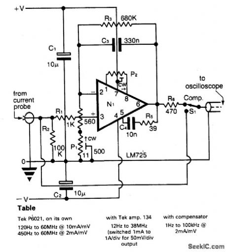
Circuit Notes
A clamp-on“current probe such as the Tektronix P6021 is a useful means of displaying current waveforms on an oscilloscope. Unfortunately, the low-frequency response is somewhat limited, as shown in the Table.The more sensitive range on the P6021 is 2 mA/mV, but it has a roll-off of 6 dB per octave below 450 Hz. The compensator counteracts the low-frequency attenuation, and this is achieved by means of C3 and R4 + P1 in the feedback around op amp N1.The latter is a low-noise type, such as the LM725 shown, and even so it is necessary at some point to limit the increasing gain with decreasing frequency; otherwise amplifier noise and drift will overcome the signal. The values shown for C3R3 give a lower limit below 1 Hz. A test square wave of ±10mA is fed to the current probe so that P1 can be adjusted for minimum droop or overshoot in the output waveform. At high frequencies, the response begins to fall off at 100 kHz. (View)
View full Circuit Diagram | Comments | Reading(1528)
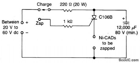
Ni_CAD_BATTERY_ZAPPER_II
Published:2009/7/3 4:01:00 Author:May
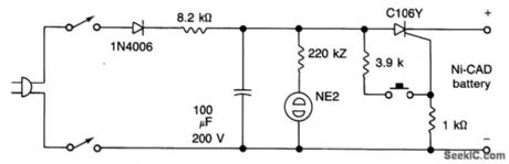
This zapper clears intemal short in nickel cadmium batteries by buming it away. CAUTION: The negative battery terminal is connected to one side of the ac line. For safety operation use a 1:1 isolation transformer. (View)
View full Circuit Diagram | Comments | Reading(864)
LEVEL_SHIFT_WITH_IC
Published:2009/7/3 4:00:00 Author:May
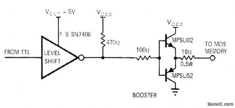
Level shifter for dynamic MOS random-access memory uses SN7406 IC with two-transistor booster to convert TTL levels to MOS levels. Booster can be omitted for data input lines because they drive such low capacitive loads in typical arrays.-M.E. Hoff, Designing an LSI Memory System That Outperforms Cores-Economically, Computer Hardware (section of EDN Magazine), Jan. 15, 1971, p 6-15 (p 000110-001111). (View)
View full Circuit Diagram | Comments | Reading(1819)
THERMALLY_CONTROLLED_Ni_CAD_CHARGER
Published:2009/7/3 4:00:00 Author:May
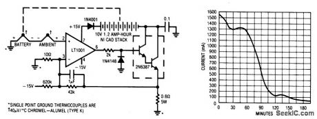
One way to charge Ni-Cad batteries rapidly without abuse is to measure cell temperature and taper the charge accordingly. The circuit uses a thermocouple for this function. A second thermocouple nulls out the effects of ambient temperature. The temperature difference between the two thermocouples determines the voltage which appears at the amplifier's positive input. As battery temperature rises, this small negative voltage (1℃ difference between the thermocouples equals 40 μV) becomes larger. The amplifier, operating at a gain of 4300, gradually reduces the current through the battery to maintain its inputs at balance. The battery charges at a high rate until heating occurs and the circuit then tapers the charge. The values given in the circuit limit the battery surface temperature rise over ambient to about 5℃. (View)
View full Circuit Diagram | Comments | Reading(495)
LITHIUM_BATTERY_CHARGER
Published:2009/7/3 3:59:00 Author:May
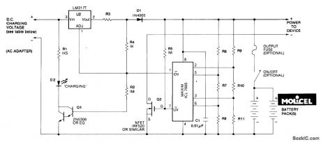
Charging is accomplished with a constant current of 60 mA for AA cells to a cutoff voltage of 2.4 V per cell at which point the charge must be terminated. The charging system shown is designed for multi-cell battery packs of 2 to 6 series-connected cells or series/parallel arrangements. It is essential that all cells assembled in the pack be at an identical state-of-charge (voltage) prior to charging. The maximum upper cut-off voltage is 15.6 volts (6 x 2.6 V). (View)
View full Circuit Diagram | Comments | Reading(2110)
Ni_CAD_BATTERY_ZAPPER
Published:2009/7/3 3:57:00 Author:May
The short in a Ni-Cad battery can be burned off with this zapper. Use of the SCR keeps heavy discharge current from damaging switch contacts. (View)
View full Circuit Diagram | Comments | Reading(666)
GEL_CELL_CHARGER
Published:2009/7/3 3:56:00 Author:May
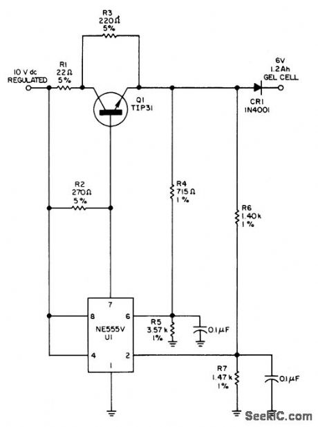
This circuit detects a full-charge state andautomatically switches to a float condition-from240 mA to 12 mA. (View)
View full Circuit Diagram | Comments | Reading(533)
AUDIBLE_TUNING_FOR_BLIND
Published:2009/7/3 3:51:00 Author:May
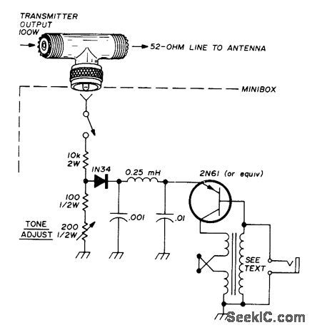
Transmitter or exciter output is sampled at coax line and highresistance voltage divider. Rectified voltage of divider, which varies during transmitter tuning, is fed to relaxation oscillator whose output varies in pitch with voltage; low voltage gives high-pitched tone, and high voltage gives lowpitched tone. Input divider draws about 1 W from 100-W transmitter; for higher power, such as 1 kW, change 10K to about 100K. Diode feeds about 2 V to emitter of transistor. Any audiotype PNP transistor can be used. For NPN device, reverse diode connections. Transformer is from 5-W transistor amplifier, with 22-ohm high-impedance winding. Other two windings, in series aiding, are 4 ohms each.-D.H. Atkins, Tuning Aid for the Sightless, Ham Radio, Sept.1976, p 83 (View)
View full Circuit Diagram | Comments | Reading(562)
SCA_DEMODULATOR_
Published:2009/7/3 3:48:00 Author:May
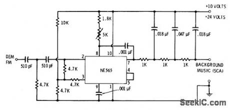
VCO of NE565 PLL is set at 67 kHz and is locked in by incoming 67-kHz subsidiary-carrier component used for transmitting unintewupted commercial background music by FM broadcast stations. Circuit demodulates FM sidebands and applies them to audio input of commercial sound system through suitable filter. 5K pot is used to lock VC0 exactly on frequency. Frequency response extends up to 7000 Hz.-E. M. Noll, Linear IC Principles, experiments, and Proiects, Howard VV. Sams, Indianapolis, IN, 1974, p 212-213. (View)
View full Circuit Diagram | Comments | Reading(1151)
AUTOMATIC_HEADLIGHT_DIMMER
Published:2009/7/3 3:47:00 Author:May
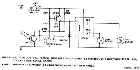
This circuit switches car headlights to the low beam state when it senses the lights of an on-coming car. The received light is very low level and highly directional, indicating the use of a lens with the detector. A relatively large amount of hysteresis is built into the circuit to prevent flashing lights. Sensitivity is set by the 22 megohm resistor to about 0.5 ft. candle at the transistor (0.01 at the lens), while hysteresis is determined by the R1, R2 resistor voltage divider, parallel to the D41K3 collector emitter, which drives the 22 megohm resistor; maximum switching rate is limited by the 0.t μF capaci-tor to 15/minute. (View)
View full Circuit Diagram | Comments | Reading(2586)
N_PHASE_MOTOR_DRIVERS
Published:2009/7/3 3:43:00 Author:May
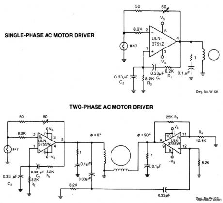
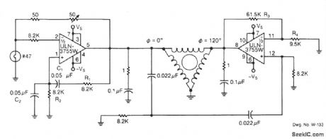
Because of its high amplification factor and built-in power-output stage, an integrated power operational amplifter makes a convenient driver for ac motors. One op amp can be configured as an oscillator to generate the required ac signal. The power-output stage, of course, supplies the high-current drive to the motor. The controlling op amp is configured as a Wein bridge oscillator. The R1C1, R2C2 feedback networks determine the oscillation frequency, according to the following expression:
By varying either R1 or R2, the oscillator frequency can be adjusted over a narrow range.The R3/R4 ratio sets the second amplifier's gain to compensate for signal attenuation occurring in the phase shifters. The circuits can be driven from an external source, such as a pulse or square wave, setting the gain of the left-hand amplifier to a level less than that required for oscillation. The RC feedback networks then function as an active ftlter causing the outputs to be sinusoidal. (View)
View full Circuit Diagram | Comments | Reading(732)
160_METER_BANDPASS
Published:2009/7/3 3:43:00 Author:May
Four-resonator filter is tunable from 1.8 to 2 MHz and has insertion loss of 5 dB.3-dB bandwidth is 30 kHz,and 6-60 dB shape factor is 4.78.Stopband attenuation is over 120 dB.Key to high performance is ward,Bandpass Filters for Receiver Preselecconstruction,and adjustment.-W. Hayward,Bandpass Filter for Receiver Preselectors,Ham Radio,Feb,1975,p 18-27. (View)
View full Circuit Diagram | Comments | Reading(861)
NARROW_BAND_DEMODULATOR_
Published:2009/7/3 3:42:00 Author:May
Low-cost TTL ICs are connected to form phase-locked Ioop narrow-band FM demodulator. With value shown for C, circuit is suitable for IF value around 470 kHz. Article covers advantages of synchronous detection and various direct conversion techniques involving phase-locked loop.-P. Hawker、 synchronous Detection in Radio Reception, Wireless World, Nov.1972,p 525-528 (View)
View full Circuit Diagram | Comments | Reading(565)
BANDPASS_FOR_CW
Published:2009/7/3 3:42:00 Author:May
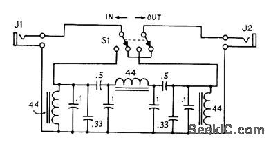
Provides bandwidth of about 400 Hz (3 dB down) centered on 875 Hz, for improving reception of CW signals with amateur receiver. Uses three 44-mH toroids.-D. C.Rife, Low-Loss Passive Bandpass CW Filters, QST, Sept. 1971, p 42-44. (View)
View full Circuit Diagram | Comments | Reading(0)
| Pages:280/471 At 20261262263264265266267268269270271272273274275276277278279280Under 20 |
Circuit Categories
power supply circuit
Amplifier Circuit
Basic Circuit
LED and Light Circuit
Sensor Circuit
Signal Processing
Electrical Equipment Circuit
Control Circuit
Remote Control Circuit
A/D-D/A Converter Circuit
Audio Circuit
Measuring and Test Circuit
Communication Circuit
Computer-Related Circuit
555 Circuit
Automotive Circuit
Repairing Circuit