
Basic Circuit
Index 279
2500_V_isolated_5_driver_5_receiver_RS_232_transceiver
Published:2009/7/23 22:48:00 Author:Jessie
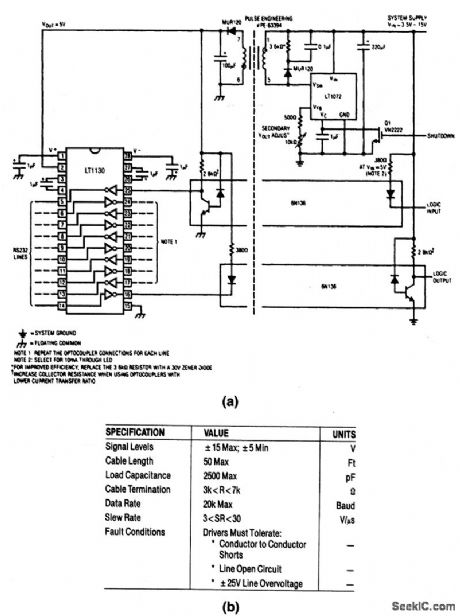
This circuit provides 2500-V isolation with optically coupled data lines, and an isolated 5-V supply. A powered transceiver eliminates the need for three supplies on both sides of the isolation transformer. The circuit meets the key RS-232 transceiver specifications (EIA RS232C.V28) shown in Fig. 6-68B. (View)
View full Circuit Diagram | Comments | Reading(556)
Power_supply_monitor
Published:2009/7/23 22:30:00 Author:Jessie
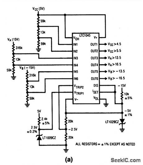
This circuit shows an LTC1045 used as a power-supply monitor. The outputs of three power supplies are tied to the positive inputs through an appropriate resistive voltage divider. The divider ratio is set so that the voltage into the comparator (Fig. 6-61B) equals the reference on the inverting input when the power-supply voltage is at a critical level. (View)
View full Circuit Diagram | Comments | Reading(2878)
Microprocessor_interface_for_free_running_A_D
Published:2009/7/23 22:39:00 Author:Jessie
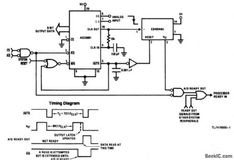
This circuit provides for asynchronous reads of analog data to an 8-bit microprocessor. The CD4024BC ripple counter generates a READY signal to the microprocessor that prevents a READ during a data update. The output data latches are updated one A/D-clock period before the INTR falls low, and the free-running conversion time is always 72 clock periods long. To start the A/D converter, a logic low must be applied to the SYSTEM RESET. The timing diagram shows relationships of the INTR, READY, and RDsignals. (View)
View full Circuit Diagram | Comments | Reading(629)
Isolated_switching_regulator_for_LAN
Published:2009/7/23 22:42:00 Author:Jessie

This power supply is suitable for local area networks, such as EthernetTM or CheapernetTM. Figure 6-65B tabulates the design specifications, based on IEEE 802.3 and ECMA 200-V. (View)
View full Circuit Diagram | Comments | Reading(483)
Data_acquisition_IC_with_4_wire_microprocessor_interface
Published:2009/7/23 22:24:00 Author:Jessie
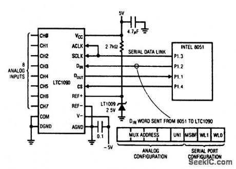
This circuit shows the basic interface connections between an 8-input LTC1090 data-acquisition IC and an Intel 8051 microprocessor.The 4-wlre serial interface includes chip-select CS, shift clock SCLK for synchronizing data bits, a data input DIN and a data output, DOUT. Data bits are transmitted and received simultaneously (full duplex), minimizing the transfer time. The external ACLK input controls the conversion rate, and can be tied to the SCLK, as shown, or can be derived from the system clock (the 8051 ALE pin), or it can be run asynchronously. When the ACLK pin is driven at 2 MHz, the conversion time is 22 μs. Consult the LTC1090 datasheet for further data. (View)
View full Circuit Diagram | Comments | Reading(985)
Programmable_power_supply_negative_output
Published:2009/7/23 22:33:00 Author:Jessie
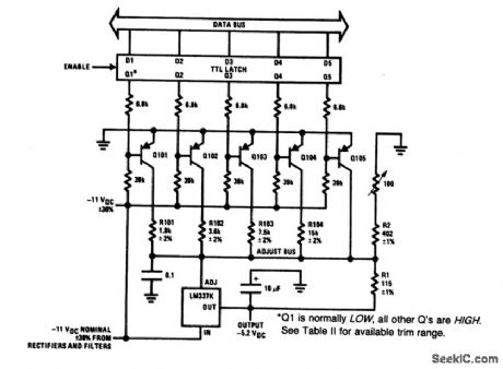
This circuit is similar to that of Fig. 6-62, except that the output is are shown in Fig. 6-63. To calibrate, apply 0111 to TTL latch, and adjust P1 for 5.200-V output. (View)
View full Circuit Diagram | Comments | Reading(496)
Programmable_power_supply
Published:2009/7/23 22:32:00 Author:Jessie
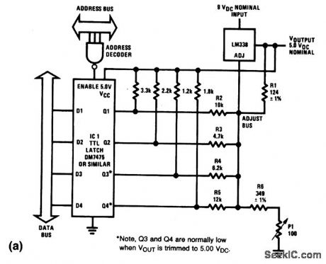
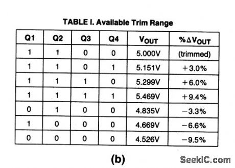
The output of this 5-V digital supply can be trimmed above and below 5-V with digital-logic signals applied to IC1. The exact values for various combinations of logic signals are given in Fig. 6-62B. To calibrate, apply 1100 to IC1, and adjust P1 for 5.000-V output. (View)
View full Circuit Diagram | Comments | Reading(1579)
Single_supply_RS_232_interface_for_bipolar_A_D_converters
Published:2009/7/23 22:46:00 Author:Jessie
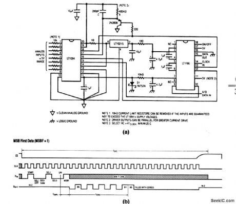
This circuit operates from a single 5-V supply, and draws a total quiescent current of about 37 mA. Figure 6-67B shows the operating sequence. The CS signal switches to a low state less than 1 μs after receiving the system clock, and the word can be transmitted after one cycle. After the 18 clock cycles required to complete conversion, the clock must shut off to allow CS to switch to a high state for at least 2 μs (minimum time between conversions). The operating sequence can then be repeated. (View)
View full Circuit Diagram | Comments | Reading(474)
RS_232_transceiver_with_automatic_power_shutdown
Published:2009/7/23 22:44:00 Author:Jessie
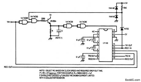
This circuit automatically shuts down when there is no data flow through the interface. A data stream on either the RS-232 or logic inputs activates the transceiver. The data must begin with a logic-1 preamble, and the data stream must contain a sufficient number of 1s to keep the transceiver active. The preamble can be as short as 50 μs. Alternatively, input to the circuit could be an RS-232 handshake signal, such as Data Set Ready (DSR) or Clear to Send (CTS), which remain high during the data transfer. The LT1180 200-μs turn-on delay does not limit the data rate in the circuit. Once the LT1180 is active, data can be processed at the maximum 100kbaud data rate. (View)
View full Circuit Diagram | Comments | Reading(580)
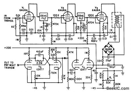
PULSED_30_W_TRANSMITTER
Published:2009/7/23 23:03:00 Author:Jessie
Uses pulsed Hartley oscillator operating at either 85 or 135 kc, followed by push-pull driver amplifier, push-pull power amplifier, and power amplifier that feeds 72-ohm transducer through step-down transformer Q1. Oscillator operates for 1-millisec period controlled by V1, which in turn is triggered by negative pulse coming from receiver through free-running mvbr V6.-H. F. Messias, UItrasonics Measures Flow Velocity of Rivers, Electronics, 34:41, p 56-59.
(View)
View full Circuit Diagram | Comments | Reading(496)
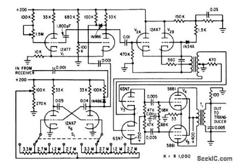
TRF_RECEIVER
Published:2009/7/23 23:01:00 Author:Jessie
Operates at either 85 or 135 kc. Input impedance is 72 ohms to match transducer. Detected pulse of rectifier bridge is amplified in direct. coupled amplifier V4 and differentiated at its output, to trigger one-shot mvbr V5, which in turn triggers Transmitter and prf multiplier in computing circuitry.-H. F. Messias, Ultrasonics Meassures Flow Velocity of Rivers, Electronics, 34:41, p 56-59. (View)
View full Circuit Diagram | Comments | Reading(579)
QUADRATURE_VOLTAGE_REJECTION
Published:2009/7/23 23:21:00 Author:Jessie
Suppresses quadrature voltages in servo loops while delivering in-phase a-c signal. Phase reference voltage controls two unmatched diodes so they conduct only when in-phase signal component is passing through maximum and quadrature is passing through minimum. Prevents overload of amplifier.-B. Fennick, Phase-Selective Gate Rejects Quadrature, Electronics, 31:51, p 89-91. (View)
View full Circuit Diagram | Comments | Reading(494)
BATTERY_STATUS_INDICATOR
Published:2009/7/3 4:22:00 Author:May

Continually monitors battery voltage during use and consumes only about 250 pA (until the end point is reached). Near the end point Tr1 turns off, allowing Tr2 to illuminate the LED to increase current drain further leading to a distinct turn off point. (View)
View full Circuit Diagram | Comments | Reading(1863)
VOLTAGE_DETECTOR_RELAY_FOR_BATTERY_CHARGER
Published:2009/7/3 4:21:00 Author:May

While the battery is being charged, its voltage is measured at V. If the measured voltage is lower than the minimum the relay will be energized, that will connect the charger circuit. When the battery voltage runs over the maximum set point, the relay is deenergized and it will be held that way until the voltage decreases below the minimum when it will be connected again. The voltage is lower than a threshold VB (low breaking voltage) the relay will be assumed that such a low voltage is due to one or several dam-aged battery components. Of course VB is much lower than the minimum set point. (View)
View full Circuit Diagram | Comments | Reading(886)
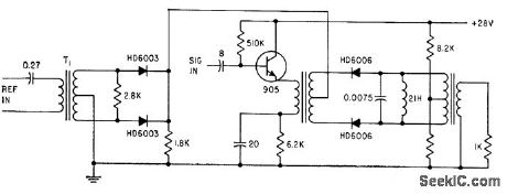
GARRIER_SYSTEM_RECEIVER_
Published:2009/7/3 4:21:00 Author:May

Used to detect,amplify,limit,and demodulate FM carrier modulated with audio ρrogram、for feeding up to 2.5 W to remote loudspeaker. Can be plugged into any AC outlet on same side of distribution transtormer. Carrier signal is taken lrom line by tuned transtormerr,. Output of two-stage Iimiter amplifier Q1A-Q1D is applied directlv to mute peak detector D1-Q2-C7. Limiter output is reduced to1 V P-P for driving National LM565CN PLL detector which operates as narrow-band tracking filter for input signal and provides low-distortion demodulated audio output. Mute circuit quiets receiver in absence of carrier.-J. Sherwin, N. Sevastopoulos, and T, Regan, FM Remote Speaker System, National Semiconductor, Santa Clara, CA, 1975, AN-146. (View)
View full Circuit Diagram | Comments | Reading(837)
LATCH_MEMORY
Published:2009/7/3 4:18:00 Author:May
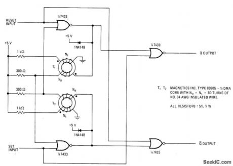
Use of saturable transformers makes memory nonvolatile and immune to false command signals. Transformers stay magnetically biased without voltage supply to provide reference state to which memory latch retumswhen power is reapplied. When bit is initially stored in circuit, set or reset pulse must have minimum width of 35 μs and minimum separation of 65 μs.-G. E. Bloom, Saturable Core Transformers Harden Latch Memories, Electronics, March 31, 1977, p 104-105. (View)
View full Circuit Diagram | Comments | Reading(783)
1_kHz_FIFTH_ORDER_LOW_PASS
Published:2009/7/3 4:15:00 Author:May

Used with 1-kHz signal generator to remove unwanted harmonics,leaving pure sine wave as required formeasuring distortion in modern audio amplifiefs Attenuation peaks are carefuny positionedto coincide with second and third harmonics,giving 65-dB attenuation of these harmonicsand at least 50-dB attenuation of higher hatmonics.-J A,Hardcastle,1 kHz Source Cleaning Filter,Wireless World,Oct,1978,p 59. (View)
View full Circuit Diagram | Comments | Reading(0)
PROM_POWER_DOWN
Published:2009/7/3 4:15:00 Author:May
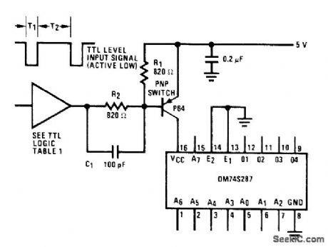
Conserves power in applications when data is required from PROM for only small percentage of system cycle. Circult turns PROM off automatically when not needed, with access time increased only by 80-ns delay of power-down circuit. PNP switch can be PN4313 or 2N3467 pass transistor. With two 74S04 sections in series at input, active low selection is obtained. 74S00 at input gives active high selection. When logic input to R2 goes low, PNP switch is turned on and +5V is applied to National DM74S287 256 x 4 PROM.- Memory Applications Handbook, National Semiconductor, Santa Clara, CA, 1978, p 5-9-5-12. (View)
View full Circuit Diagram | Comments | Reading(817)
VOICE_BANDPASS
Published:2009/7/3 4:14:00 Author:May

Used between 8-ohm output of communication receiver and 8-ohm Loud-speaker or low-impedance phones, to suppress Continuous Random Unwanted Disturbances on voice transmissions. Passband is 355 to 2530 Hz at 3-dB points. L1 and L3 are 4a-mH toroids.L2 is 88-mH toroid with 94 turns removed. T1 and T2 are 88-mH toroids with 100 turns No.28 enamel wound over original winding of each for primary.-R. M. Myers, The SSB Crud-O-Ject, QST, May 1974, p 23-25 and 56 (View)
View full Circuit Diagram | Comments | Reading(1302)
2955_MHz_HIGH_PASS
Published:2009/7/3 4:13:00 Author:May

Used in offset frequency-measuring system for amateur-band signals. Nine-section Chebvshev high-pass filter with 1-dB passband ripple attenuates undesired 2.045-2.245 MHz image 16 dB while selecting desired 2.955-3.155 MHz signal. Filterhas sharper cutoff characteristic, for given num ber of sections, than Butterworth or image parameter designs.-J. Walker, Accurate Frequency Measurement of Received Signals, Ham Radio, Oct. 1973, p 38-55. (View)
View full Circuit Diagram | Comments | Reading(653)
| Pages:279/471 At 20261262263264265266267268269270271272273274275276277278279280Under 20 |
Circuit Categories
power supply circuit
Amplifier Circuit
Basic Circuit
LED and Light Circuit
Sensor Circuit
Signal Processing
Electrical Equipment Circuit
Control Circuit
Remote Control Circuit
A/D-D/A Converter Circuit
Audio Circuit
Measuring and Test Circuit
Communication Circuit
Computer-Related Circuit
555 Circuit
Automotive Circuit
Repairing Circuit