
Basic Circuit
Index 266
5_30_V_AT_15_A
Published:2009/7/6 2:11:00 Author:May
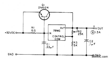
External series-pass transistor boosts 500-mA rated output of 78MG or 79MG regulator to 1.5 A for use as adiustable power supply in lab. Circuit has no short-circuit protection for safe-area limiting for external pass transistor, but article shows how to add protective transistor for this purpose.-J. Tru-Iove, A New Breed of Voltage Regulators, 73 Magazine, March 1977, p 62-64. (View)
View full Circuit Diagram | Comments | Reading(1709)
_50_V_FLOATING
Published:2009/7/6 2:10:00 Author:May

RCA CA723 regulator operating from 85-V supply delivers 50 V with Iine regulation of 15 mV for 20-V supply change and load regulation of 20 mV for 50-mA load current change.- Linear Integrated Circuits and M0S/ FET' s, RCA Solid State Division, Somerville, NJ, 1977, p 61. (View)
View full Circuit Diagram | Comments | Reading(879)
High_performance_supervisory_circuit
Published:2009/7/23 21:30:00 Author:Jessie
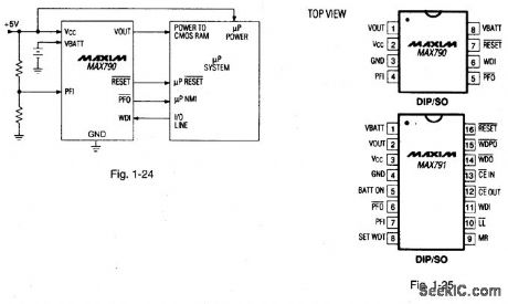
Figures 1-24 and 1-25 show a typical application circuit and pin configurations, respectively, for the MAX790/791. The IC is similar to the MAX690 series (Figs. 1-14 and 1-15), but with several improvements, including 70-μA supply current, 10-ns CE propagation delay, 250-mA output current (VCC mode), and 25-mA output current (VBATT mode). The MAX790 is pin compatible with the MAX690. The reset output is guaranteed to be in the correct state for VCC down to 1 V. MAXIM NEW RELEASES DATA BOOK, 1992, P. 5-53. (View)
View full Circuit Diagram | Comments | Reading(566)
Basic_bipolar_output_DAC
Published:2009/7/23 21:29:00 Author:Jessie

This circuit shows a DAC that is connected for bipolar-output D/A-converter operation. (View)
View full Circuit Diagram | Comments | Reading(676)
Microprocessor_supervisory_circuit_added_features
Published:2009/7/23 21:28:00 Author:Jessie


Figures 1-17 and 1-18 show a typical application circuit and pin descriptions, respectively for a MAX696. The IC is similar to that described for Figs. 1-J through 1-N, but with added (or combined) features. Use the equations shown in Fig. 1-M to calculate the values for the resistors at the PFI and LLIN inputs (except use a threshold of 1.3 V, instead of 2.54 V). Figures 1-19, 1-20, 1-21, 1-22, and 1-23 show the reset timing, watchdog and reset timeout selection, calculations and connections for adding hysteresis, circuit for disabling the watchdog under program control, and circuit for selecting watchdog timeout, respectively. Table 1 in Fig. 1-18 refers to Fig. 1-20 in this book. Figure 1 in Fig. 1-18 refers to Fig. 1-17 in this book. Figure 5 in Fig. 1-18 refers to Fig. 1-19 in this book. Figure 7 in Fig. 1-18 refers to Fig. 1-21 in this book. Figure 2 in Fig. 1-18 is an internal function not shown here. MAXIM NEW RELEASES DATA Book, 1992, P. 5-36, 5-37, 5-41, 5-43. (View)
View full Circuit Diagram | Comments | Reading(556)
COLLECTOR_TRIGGERED_FLIP_FLOP
Published:2009/7/23 21:28:00 Author:Jessie

Diodes with basic flip-lop serve as steering circuit,with negative input pulse being used to trigger collectors. Maximum trigger rate exceeds 5 Mc with trigger amplitude from 4 to 12 v.- Transistor Manual, Seventh Edition, General Electric Co., 1964, p 197. (View)
View full Circuit Diagram | Comments | Reading(589)
Basic_unipolar_negative_reference__DAC
Published:2009/7/23 21:27:00 Author:Jessie

This circuit shows a DAC that is connected for unipolar negative-reference D/A-converter operation. (View)
View full Circuit Diagram | Comments | Reading(449)
Low_cost_supervisory_circuit_with_battery_backup
Published:2009/7/23 21:34:00 Author:Jessie

Figures 1-30 and 1-31 show a typical application circuit and pin configurations, respectively, for the MAX703/MAX704. The ICs are similar to that described for Figs. 1-J through 1-M, but with generally lower cost. The ICs have a 200-ms reset pulse width, 200-μA quiescent current, 50-nA quiescent with battery backup, and a 1.25-V threshold detector for power-fail warning, low-battery detection, or for monitoring a power supply voltage other than +5 V. MAXIM HIGH-RELIABILITY DATA Book, 1993, P. 5-29 (View)
View full Circuit Diagram | Comments | Reading(576)
Microprocessor_supervisory_circuit_high_reliability_added_features)
Published:2009/7/23 21:33:00 Author:Jessie

Figures 1-28 and 1-29 show a typical application circuit and pin configurations, respectively, for the MAX691 A /693A /800L / 800M. The ICs are similar to that described for Figs. 1-J through 1-M, but with more reliability and added features.The ICs improve performance with 35-μA supply current, 200-ms typical reset delay on power-up, and 6-ns chip-enable propagation delay. Other features include write protection of CMOS RAM or EEPROM, separate watchdog outputs, battery-backup switchover, and a reset output that is valid with VCC down to 1 V.The MAX691A/MAX800L have a 4.65-V typical reset-threshold. The MAX693A/ MAX800M reset threshold is 4.4V (typical). The MAX800L/MAX800M is guaranteed to deliver power-fail accuracies to 12%. MAXIM HIGH-RELIABILITY DATA Book, 1993, P. 5-19. (View)
View full Circuit Diagram | Comments | Reading(794)
Microprocessor_supervisory_circuit_high_reliability
Published:2009/7/23 21:31:00 Author:Jessie

Figures 1-26 and 1-27 show a typical application circuit and pin configurations, respectively, for the MAX690A/MAX802L. The ICs are similar to that described for Figs. 1-J through 1-N, but with added reliability and other reset thresholds. The MAX690A/MAX802L generate a reset pulse when the supply drops below 4.65V, and the MAX692A/MAX802M generate a reset below 4.40 V. The threshold is 1.25V for both power-fail warning and low-battery detection. The reset delay is 200 ms. The watchdog timer has a 1.6-s timeout. Quiescent current is 200μA with normal power and 50nA in battery-backup mode. The power-fail accuracy is ±2% for MAX802L/M. MAXIM HIGH-RELIABILITY DATA Book, 1993, P. 5-17. (View)
View full Circuit Diagram | Comments | Reading(576)
LOW_COST_BASIC_SCHMITT
Published:2009/7/23 21:30:00 Author:Jessie

Developed for use with inexpensive 2N711 germanium pnp mesa switching transistors. Can serve as source of 10-Mc square waves, as pulse restorer, or as general-purpose square wave generator.-P. A. Mclnnis, Low-Cost Computer Circuits, Motorola Application Note AN-130, Nov. 1965. (View)
View full Circuit Diagram | Comments | Reading(623)
Offset_binary_D_A_converter_operation
Published:2009/7/23 21:30:00 Author:Jessie

This circuit shows a DAC/op-amp combination that is used to provide offset-binary operation. (View)
View full Circuit Diagram | Comments | Reading(726)
REGULATED_DIVIDER_FOR_±5V
Published:2009/7/6 2:10:00 Author:May

Used at output of adjustable regulated power supply providing up to 15 V, to give lower positive and negative voltages that remain steady despitechanges in load current To get +5 V and -5V from +10 V, set R1 at midposition and adjust R2 for 20 mA through output transistors,Uses 741 opamp.-C.H. Banthorpe、 Voltage Divider, Wireless world, Doc 1976,p41 (View)
View full Circuit Diagram | Comments | Reading(1529)
COUNTER_DRIVE_FOR_WWVB
Published:2009/7/6 2:09:00 Author:May

Uses LM311 as true zero-crossing detector for 60-kHz carrier of NBS standard-frequency station at Boulder, Colorado. Resulting square wave is fed to chain of 7490 dividers whose outputs are selected by S2 to serve as gate for frequency counter.T1 is 24-V 500-mA power transformer, and T2 is 40-kHz cupcore slugtuned RF transformer as used in many TV remote controls. Primary inductance (7.5-46 mH) of T2 is tapped at 0.5 mH;secondary is 20 pH. Article also gives circuit of preamp that can be built into 60-kHz loop antenna to build up signal strength to 0.4 V as re quired for input to processor.-H. Isenring, WWVB Signal Processor, Ham Radio, March 1976, p 28-34.
(View)
View full Circuit Diagram | Comments | Reading(2272)
4_bit_D_A_converter_with_microprocessor_interface
Published:2009/7/23 21:43:00 Author:Jessie

This circuit uses a DAC-4888 and a few external components to form a D/A converter with microprocessor interface (4-bit data bus). The output is + 10 V to -10 V with complementary binary input (all zeros equal full scale). (View)
View full Circuit Diagram | Comments | Reading(716)
Basic_comparator_with_hysteresis
Published:2009/7/23 21:43:00 Author:Jessie

This circuit uses one section of a 3403 op amp as a comparator (without the use of an IC comparator). (View)
View full Circuit Diagram | Comments | Reading(753)
25_250_MHz_PRESCALER
Published:2009/7/6 2:08:00 Author:May

Based on use of Fairchild 95H90 decade counter, with preamp Q1 and associated components selected for 25-250 MHz range. 1N914N diodes prevent over-loading of input. Voltage regulator is LM340T-5, L1 is 8 tums No. 28 wound on body of 1000-ohm or larger 1/2-W resistor, with ends soldered to resistor leads. Quarter.wave whip antenna at inputwill pick up adequate signal from 1-W 146-MHz transceiver hand-held 6-10 feet away.Counter provides division by 10.-R. D. Shriner, Prescaler Updates the DVM/Frequency Counter, QST, Sept. 1978, p 22-24 and 37. (View)
View full Circuit Diagram | Comments | Reading(2796)
SINGLE_CONVERSION_SYNTHESIZER
Published:2009/7/6 2:07:00 Author:May

Used in single-conversion CB transceiver in whichVCO operates at channel frequency during transmit and 455 kHz below channel frequency during receive. 5.120 MHz is quintupled to 25.600 MHz to mix and provide input to programmable divider.-L.Sample,A Linear CB Synthesizer, IEEE Transactions on Consumer Electronics Aug,1977、p 200-206 (View)
View full Circuit Diagram | Comments | Reading(630)
Power_supply_monitor_with_reset
Published:2009/7/23 21:40:00 Author:Jessie


Figures 1-43, 1-44, and 1-45 show a typical application circuit, pin configuration, and pin descriptions, respectively, for the MAX709, The IC provides a system reset during power up, power down and brownout conditions. When VCC falls below the reset threshold (Fig. 1-46), RESET becomes low and holds the microprocessor for 140 ms (minimum) after VCC rises above the threshold. The RESET output is guaranteed to be in the correct state with VCC down to 1 V. The IC is relatively immune to short-duration negative-going VCC transients (glitches), as shown in Fig. 1-47. Figure 1-48 shows the addition of R1 when the RESET output must be valid down to 0 V. The value of R1 should be about 100 kΩ, but it is not critical. Figure 1-49 shows the circuit for interfacing to microprocessors with bidirection reset pins (such as the Motorola 68HC11 series). MAXIM NEW RELEASES DATA BOOK, 1994, P. 5-67, 5-70, 5-71. (View)
View full Circuit Diagram | Comments | Reading(555)
16_bit_D_A_converter_with_microprocessor_interface
Published:2009/7/23 21:40:00 Author:Jessie

This circuit uses a DAC-4881 and a few external components to form a D/A converter with microprocessor interface (16-bit data bus). The output is 0 to -4 mA with straight binary input and an external reference. (View)
View full Circuit Diagram | Comments | Reading(629)
| Pages:266/471 At 20261262263264265266267268269270271272273274275276277278279280Under 20 |
Circuit Categories
power supply circuit
Amplifier Circuit
Basic Circuit
LED and Light Circuit
Sensor Circuit
Signal Processing
Electrical Equipment Circuit
Control Circuit
Remote Control Circuit
A/D-D/A Converter Circuit
Audio Circuit
Measuring and Test Circuit
Communication Circuit
Computer-Related Circuit
555 Circuit
Automotive Circuit
Repairing Circuit