Basic Circuit
MEDIUM_POWER_INVERTER
Published:2009/7/7 9:36:00 Author:May | From:SeekIC

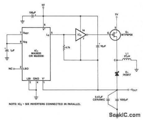
In this circuit, a CMOS inverter, such as the CD4069, is used to convert the open drain L, output to a signal suitable for driving the gate of an external P MOSFET The MTP8P03 has a gate threshold voltage of 2.0 V to 4.5 V, so it will have a relatively high resistance if driven with only 5 V of gate drive. To increase the gate drive voltage, and thereby increase efficiency and power handling capability, the negative supply pin of the CMOS inverter is connected to the negative output, rather than to ground. Once the circuit is started, the P MOSFET gate drive swings from + 5 V to - VOUT . At start up, the - VOUT is one Schottky diode drop above ground and the gate drive to the power MOSFET is slightly less than 5 V. The output should be only lightly loaded to ensure start up, since the output power capability of the circuit is very low until - VOUT is a couple of volts.This circuit generates complementary output signals from 50 to 240 Hz. Digital timing control ensures a separation of 10 to 15° between the fall time of one output and the rise time of the complementary out-put.The digital portion of inverter U1 to U4 controls the drive to Q1 and Q2, both MTE60N20 TMOS devices. These devices are turned on alternately with 11.25°separation between complementary out-puts. A +12-V supply for CMOS gates U1 to U4 is developed by T1, D3, D4, C7, and U6. The power supply for the TMOS frequency generator is derived from the diode bridge, U5, and capacitor C7; it is applied to the center tap of T2.
Reprinted Url Of This Article:
http://www.seekic.com/circuit_diagram/Basic_Circuit/MEDIUM_POWER_INVERTER.html
Print this Page | Comments | Reading(3)

Article Categories
power supply circuit
Amplifier Circuit
Basic Circuit
LED and Light Circuit
Sensor Circuit
Signal Processing
Electrical Equipment Circuit
Control Circuit
Remote Control Circuit
A/D-D/A Converter Circuit
Audio Circuit
Measuring and Test Circuit
Communication Circuit
Computer-Related Circuit
555 Circuit
Automotive Circuit
Repairing Circuit
Code: