
Circuit Diagram
Index 692
FM_HISS_LIMITER
Published:2009/7/13 5:59:00 Author:May

Uses low-pass filter to remove noise sometimes heard with weak passages during stereo reception of FM stations. FET driven by output of amplifier or tuner is used to switch low-pass filter into operation rather than switching over to mono. Based on fact that the hiss is an antiphase effect that can be removed with little detriment to overall signal.-G. Hibbert, Stereo Noise Limiter Improvement, Wireless World, March 1976, p 62. (View)
View full Circuit Diagram | Comments | Reading(1013)
INTEGRATING_CURRENT_METER_CIRCUIT
Published:2009/7/16 2:50:00 Author:Jessie
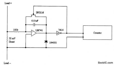
The current in the line produces a dc drop across the shunt, which feeds an integrator. When the integrator output reaches the level required to activate the Schmitt trigger, the 0.01-μF capacitor that is used in the integrator is discharged and a pulse is produced at the output of the Schmitt trigger (7414). A digital counter counts these pulses, and the counter reading is proportional to the product of current flow and time. (View)
View full Circuit Diagram | Comments | Reading(1603)
HEADPHONE_AMPLIFIER
Published:2009/7/13 5:58:00 Author:May

Designed to drive medium- to high-impedance headphones. Add matching transformers having 1000-ohm primaries if using low-impedance headphones. Dual 1-megohm pot controls gain in stereo channels over range of 1 to 100. Use 9-15 V well-filteredsupply rated at least 20 mA. Use Motorola MC3401P or National LM3900 quad opanp and 2N2924 or equivalent NPN transistor.-C. D. Rakes, Integrated Circuit Projects, Howard W. Sams, Indianapolis, IN, 1975, p 21-24. (View)
View full Circuit Diagram | Comments | Reading(0)
VIDEO_I_F_USES_FRAME_GRID_6GK7
Published:2009/7/16 2:50:00 Author:Jessie
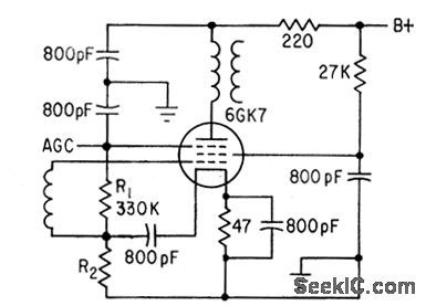
Negative voltage on suppressor controls gain of dual-control sharp-cutoff pentode. Cathode cur rent is independent of agc, and control grid bias automatically adjusts to prevent modulation clipping.-L. Solomon, New Tubes and Circuits for Consumer Electronics, Electronics, 36:2, p 47-49. (View)
View full Circuit Diagram | Comments | Reading(627)
3O_MC_TO_55_MC
Published:2009/7/13 5:55:00 Author:May

Single transistor serves as mixer to give 5.5-Mc i-f signal from 30-Mc signal input and 35.5.-Mc oscillator input.Output is 100 mv for 10-mv signal input, with 630-mv oscillator signal.-Texas Instruments Inc. Solid-State Communications, McGraw-Hill, N.Y. 1966, p300. (View)
View full Circuit Diagram | Comments | Reading(698)
VOLTAGE_TO_FREQUENCY_CONVERTER
Published:2009/7/13 5:51:00 Author:May

Q4 supplies charging current for C in relaxation oscillator Q5. Differential amplifier Q1-Q2 compares charging current with input voltage. Difference signal, amplified by Q3, controls charging current through Q4 and thus makes output frequency proportional to input voltage. For 0 to +5V input, output is 0 to 100 cps with 0.1% linearity.-W. H. Voelker, Transistor Circuit Converts Voltage to Regulated Frequency, Electronics, 37:29, p73-74. (View)
View full Circuit Diagram | Comments | Reading(0)
BRIDGE_WITH_AGC_ON_BOTH_DIODES
Published:2009/7/16 2:50:00 Author:Jessie

Agc is applied to center tap of transformer, to turn one diode off while other is being turned on. Attenuation can be 40 db over bandwidth up to 250 Mc with agc bias of 0.5 to 3 v. Insertion loss is only a few db.-W.A. Rheinfelder, Designing Automatic Gain Control Systems, EEE, 13:1, p 53-57. (View)
View full Circuit Diagram | Comments | Reading(661)
PULSE_HEIGHT_TO_TIME_CONVERTER
Published:2009/7/13 5:49:00 Author:May

Output width is proportional to input height. Last stage of constant-current charge circuit can be eliminated if output impedance can be high.-D. N. Carson and S. K. Dhawan, Data Conversion Circuits for Earth Satellite Telemetry, Electronics, 33:3, p82-84. (View)
View full Circuit Diagram | Comments | Reading(683)
SYMMETRICAL_LIMITING_RADAR_I_F_AMPLIFIER
Published:2009/7/16 2:50:00 Author:Jessie
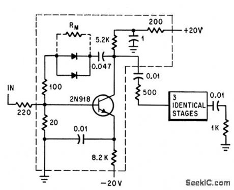
Four-stage i-f using silicon planar epitaxial transistors gives 35 db suppression of second harmonic for input of 0.3 to 30 mV. With one more stage and resistor RM across feedback diode, total phase shift is less than 25 deg.-R. F. Kirkpatrick and R. C. Stouffer, Symmetrical Limiting I-F Reduces Second Harmonic, Electronics, 37:12, p 72-73. (View)
View full Circuit Diagram | Comments | Reading(781)
D_C_TO_D_C_VOLTAGE_BOOSTER
Published:2009/7/13 5:46:00 Author:May

Depends on alternate storing and retrieving of energy from magnetic field of ringing choke. Uses blocking oscillator Q1 to chop input signal.Darlington pair Q1-Q2 provides high input impedance. Q3 is regulating transistor, and Q4 is blocking oscillator. Provides isolated 2,400 v output and 375V output.-J. F.Howell, Ringing Choke Simplifies D-C to D-C Conversion, Electronics, 39:8, p90-92. (View)
View full Circuit Diagram | Comments | Reading(947)
10_MC_SUPERREGENERATIVE_I_F
Published:2009/7/16 2:49:00 Author:Jessie
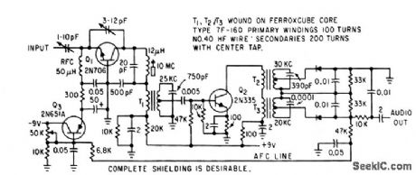
Grounded-base oscillator Q1 is self-quenched at 25 kc. Quench wave is amplified by Q2 and detected in modified Travis discriminator T2-T3.Afc voltage developed at discriminator is fed back to Q3 to maintain emitter current of Q1 at required value for quench rate.-N. H. Brown, Improved Superregenerator has Quench Converter, Electronics, 35:38, p 53. (View)
View full Circuit Diagram | Comments | Reading(1046)
ANALOG_FLUXGATE_MAGNETOMETER_ASSEMBLY
Published:2009/7/13 5:45:00 Author:May

An audio input drives the sine-wave control input, switching (or gating ) the core in and out of saturation and drawing in or releasing an external magnetic field.Weak signals at the sense outputs are proportional to field strength. (View)
View full Circuit Diagram | Comments | Reading(1271)
PLL_DETECTOR
Published:2009/7/16 2:48:00 Author:Jessie

Developed for use with BFO multiplexor in 455-kHz multimode detection system using NE561 phase-locked loop IC. Circuit provides required 90° phase-shift network in series with output of BFO multiplexor, to compensate for lockup of NE561 in quadrature with signal at input of phase detector during AM reception. IF input level to NE561 should be below about 100 mVRMS for minimum distortion. Audio output level will then be at least half that for narrow-band FM, about same for SSB and CW, and about double for AM if both sidebands are passed by IF filters. FM audio output level is proportional to percent deviation and cannot be increased by increasing signal level. Two 0.004-μF capacitors limit audio bandwidth to about 4 kHz. VCO output of NE561 is 0.6 V P-P square wave at AM carrier or BFO frequency.-J. Regula, BFO Multiplexor for a Multimode Detector, Ham Radio, Oct. 1975, p 52-55. (View)
View full Circuit Diagram | Comments | Reading(3747)
AMPLIFIED_FIELD_STRENGTH_METER
Published:2009/7/13 5:44:00 Author:May
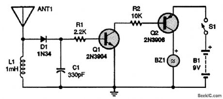
This field-strength meter uses Q1 and Q2 to amplify the dc voltage produced by detector D1. A piezo sound BZ1 is used as an audible indicator, rather than using a meter. This circuit could be of use for the visually handicapped. The antenna is a 24-in whip. (View)
View full Circuit Diagram | Comments | Reading(0)
AGC_WITH_DIODE_T_NETWORK_VARICAP
Published:2009/7/16 2:48:00 Author:Jessie

Voltage-controlled capacitor circuit minimizes effect of shunt capacitance, thus reducing resonance peaks and preventing regeneration, but insertion loss is high (8 db).-W. A. Rheinfelder, Designing Automatic Gain Control Systems, EEE, 13:1, p 53-57. (View)
View full Circuit Diagram | Comments | Reading(634)
PICOAMPERE_MEASURER
Published:2009/7/16 2:48:00 Author:Jessie
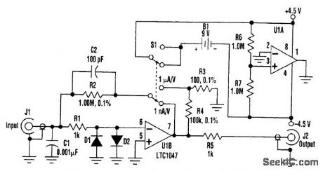
Many times, the need arises to measure current below 1 μA. The circuit shown turns any voltmeter into a picoammeter with scales of 1 μA/V and 1 μA/V. With a 3 1/2-digit voltmeter with a resolution of 1 mV, the readout will be in picoamperes or nanoamperes. In addition, it can be attached to an oscilloscope. The frequency response is about 1 kHz for the 1 μA/V setting and 150 Hz for 1 μA/V.U1B forms a transimpedance amplifier. With S1 in the position shown, the transimpedance is 1MΩ.In the other position, a gain of 1000 is added, to make the total transimpedance 1GΩ. R1, C1, D1, and D2 protect the input from high voltages, and R5 isolates the op amp's output from any load capacitance. The op amp's input current and voltage offset must be low for this circuit to work. In this case, a Linear Technology LTC1047 was used. It has a nominal input bias current of ±5 pA and a V0S of ±3μV at room temperature. U1A is used to split the 9-V battery into positive and negative supplies. The total current is essentially the supply current of the op amps. For the prototype, the total current measured for the LTC1047 was <100 μA, so a standard 9-V battery should last six months if you forget to turn it off. (View)
View full Circuit Diagram | Comments | Reading(3487)
EIGHT_PULSE_GENERATOR
Published:2009/7/13 5:43:00 Author:May
With 32-microsec gate following blocking oscillator, produces eight pulses at 4.5-microsec intervals at output of emitter-follower.-W. W. Grannemannet al. Pulse-Height-to-Digital Signal Converter, Electronics, 33:2, p58-60. (View)
View full Circuit Diagram | Comments | Reading(661)
CASCADE_I_F_WITH_AGC
Published:2009/7/16 2:48:00 Author:Jessie

Q3 is gain control element for cascade combination Q1-Q2 in 10-Mc i-f amplifier.-J. F. Perkins, Transistor Cascade Circuit Improves Automatic Gain Control in Amplifiers, Electronics, 34:22, p 49-51. (View)
View full Circuit Diagram | Comments | Reading(1058)
VOLTAGE_FREQUENCY_CONVERTER
Published:2009/7/13 5:40:00 Author:May

Linear voltage-controlled variable-frequency oscillator converts standard recorder to low.frequency f-m recorder for 0.1 to 1,000-cps signals. Values are: R1-18,000; R2-100,000; C-0.01 mfd; R-10,000; Q1-2N591; Q2-2N491; Vcc-20v; R4-270; fo-2.5 kc.-J.Schwartz, Unijunction Transistor Simplifies Voltage-Frequency Converter, Electronics, 36:43, p56. (View)
View full Circuit Diagram | Comments | Reading(1483)
30_MC_I_F_STRIP
Published:2009/7/16 2:48:00 Author:Jessie
Gain is 70 db for 3-Mc bandwidth, using 2N1405 transistors. Design equations are given.-Texas Instruments Inc., Transistor Circuit Design, McGraw-Hill, N.Y., 1963, p 276. (View)
View full Circuit Diagram | Comments | Reading(675)
| Pages:692/2234 At 20681682683684685686687688689690691692693694695696697698699700Under 20 |
Circuit Categories
power supply circuit
Amplifier Circuit
Basic Circuit
LED and Light Circuit
Sensor Circuit
Signal Processing
Electrical Equipment Circuit
Control Circuit
Remote Control Circuit
A/D-D/A Converter Circuit
Audio Circuit
Measuring and Test Circuit
Communication Circuit
Computer-Related Circuit
555 Circuit
Automotive Circuit
Repairing Circuit