
Circuit Diagram
Index 690
VOLTAGE_TO_FREQUENCY_CONVERTER
Published:2009/7/13 6:31:00 Author:May

Out-put frequency is proportional to input voltage, with 1 volt produding 1 kc. Linearity is better than 0.1%.- Transislor Manual, Seventh Edition, General Electric Co.1964, p346. (View)
View full Circuit Diagram | Comments | Reading(0)
LED_CURRENT_INDICATOR_CIRCUITS
Published:2009/7/16 2:56:00 Author:Jessie
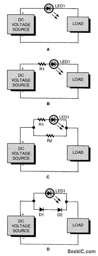
Here are some ways to connect an LED as an indicator that a load is receiving current: with the LED alone (A), with a resistor in series (B), with a resistor in series and one in parallel (C), and with two diodes in parallel (D). (View)
View full Circuit Diagram | Comments | Reading(835)
AGC_WITH_VARICAP_DIODE_BRIDGE
Published:2009/7/16 2:56:00 Author:Jessie

Uses voltage-controlled capacitors to provide very large gain control range, greater than 30 db.-W. A. Rheinfelder, Designing Automatic Gain Control Systems, EEE, 13:1, p 53-57. (View)
View full Circuit Diagram | Comments | Reading(619)
VOLTAGE_TO_PULSE_WIDTH_CONVERTER
Published:2009/7/13 6:24:00 Author:May

Converts d-c level linearly to pulse width at preset frequency. Used as switching-type series d-c regulator. C1 is selected to give desired preset frequency, and R10, R11, and R12 are chosen for desired voltage division of input.-M. C. Ellis, Linear Voltage to Duty-Cycle Converter, EEE, 12:3, p72. (View)
View full Circuit Diagram | Comments | Reading(862)
55_MC_THREE_STAGE_GERMANIUM
Published:2009/7/16 2:56:00 Author:Jessie
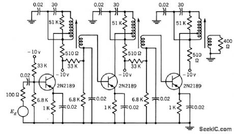
Mid-band gain is 60 db and 3-db bandwidth is 200 kc.Interstage networks consist of single-tuned transformers with collectors topped down on primary.-Texas Instruments Inc., Transistor Circuit Design, McGraw-Hill, N.Y., 1963, p 294. (View)
View full Circuit Diagram | Comments | Reading(751)
LOW_NOISE_400_MC_CONVERTER
Published:2009/7/13 6:19:00 Author:May

Voltage gain is 36 db, bandwidth 4 Mc, and noise figure only 2.5 db. Uses grounded-grid r-f and mixer stages. Applications include meteor, aurora, and forward scatter propagation studies.-L. F. Garrett, Low Noise Converter for IGY Propagation Study,ELectronics,31;5,p52-54. (View)
View full Circuit Diagram | Comments | Reading(449)
DIODE_L_ATTENUATOR_AGC
Published:2009/7/16 2:55:00 Author:Jessie

Two diodes provide maximum agc control. Circuit gives control range of about 15 db with agc voltages to 3 v. Above 200 Mc, frequency response changes irregularly with attenuation.-W. A. Rheinfelder, Designing Automatic Gain Control Systems, EEE, 13:1, p 53-57. (View)
View full Circuit Diagram | Comments | Reading(673)
COMPLEMENTARY_RAMPS
Published:2009/7/13 6:15:00 Author:May

Opamp circuit provides independent controls over amplitude and frequency, as required for amplitude-modulating auditory signals to either ear for creating impression of left to right scan. High output impedance of ramps makes use of voltage follower output stage essential. Another opamp is used for inversion and level-shifting of complementary ramp, so both ramps are available from very low impedance sources. Article describes circuit operation in detail. For values shown, ramp output is variable from 400 mV to 8V, and ramp time from 50 ms to 2 s.-L. J. Retallack, Complementary Ramp Generator with Independent Amplitude/Slope Control, Wireless World, Feb. 1975, p 94. (View)
View full Circuit Diagram | Comments | Reading(717)
10_Hz_100_kHz_RAMP
Published:2009/7/13 6:14:00 Author:May

Uses Miller integrator switched at selected rate by IC comparator in feedback loop. Ramp circuit was developed to drive FETs serving as voltage-dependent resistances in Wien-bridge oscillator of AF sweep generator. Article gives all circuits and construction details. Sweep linearity is better than 15% for all four ranges, covering 10 Hz to 100 kHz. For greatest accuracy, use 40-s sweep time; 4-s sweep is for long-persistence CRT, and 0.1-s sweep can be used only on upper three ranges.-F. H. Trist, Audio Sweep Generator, Wireless World, July 1971, p 335-338. (View)
View full Circuit Diagram | Comments | Reading(1010)
60_MC_SILICON_TETRODE_STAGE
Published:2009/7/16 2:55:00 Author:Jessie
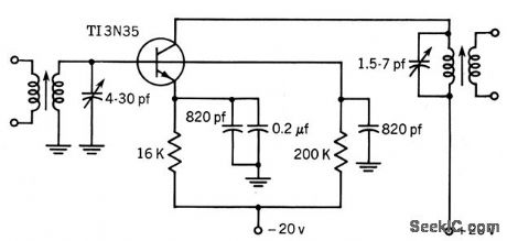
Used in eight-stage strip having identical stages except for input and output, whose transformers are designed for driving and load resistances. Transitionally coupled doubletuned interstages are used, with 5:1 mismatch providing stability and ease of alignment dong with stage gain of 12.5 db.-Texas Instruments Inc., transistor Circuit Design, McGraw-Hill, N.Y., 1963, p 292. (View)
View full Circuit Diagram | Comments | Reading(615)
30_Hz_SAWTOOTH
Published:2009/7/13 6:14:00 Author:May

Uses neons as relaxation oscillator for producing sawtooth wave required for monitor scope of SSB transmitter. Rate at which C1 charges depends on its value and those of R2 and R3. When C1 charges to breakdown voltage of neon string, around 70 V per tube, neons fire and C1 discharges through them. C1 then starts charging again, to give sawtooth output. Voltage source should be about 500VDC, and R1 at least 500K. For greater sweep width, increase number of neons in series.-D. Schmarder, A Simple Sweep Generator for Monitor Scopes, 73 Magazine, Feb. 1974, p 32. (View)
View full Circuit Diagram | Comments | Reading(635)
CONTROL_FOR_FISH_SHOCKER
Published:2009/7/16 2:55:00 Author:Jessie
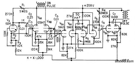
Produces liming pulses that can be varied in range of 2 to 30 cps, with durations up to 250 millisec for square waves. R1 changes frequency of oscillator V3, while C6, R4, and R5 in delay mvbr V5.V6 determine Width of pulse.-H. P. Dale, Electronic Fishing with Underwater Pulses, Electronics, 32:4, p 31-33. (View)
View full Circuit Diagram | Comments | Reading(1785)
MOS_FET_MIXER
Published:2009/7/13 6:13:00 Author:May
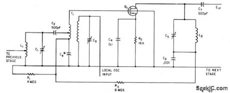
Balanced oscillator input prevents interaction between tuned circuits. Transconductance of mixer is direcdy proportional to oscillator voltage, permitting use for agc. -G. G. Luettgenau and S. H. Barnes, Designing With Low-Noise MOS FETs: A Little Different But No Harder,Electronics,37:31,p53-58 (View)
View full Circuit Diagram | Comments | Reading(1035)
FAST_FLYBACK_2_V_SAWTOOTH
Published:2009/7/13 6:13:00 Author:May

Simple modern time-base circuit using transistors can be added to old oscilloscopes that have only a synchronized free-running sweep. Size of CT determines sweep rate. When timing capacitor CT charges to breakdown voltage of reverse biased BC107B, capacitor is quickly discharged until voltage drops about 2 V and transistor assumes its high-resistance state again for start of next sweep.-K. Padmanabhan, Timebase Circuit, Wireless World, June 1974, p 196. (View)
View full Circuit Diagram | Comments | Reading(623)
ADJUSTABLE_NONLINEAR_RAMP
Published:2009/7/13 6:12:00 Author:May

Circuit provides predistortion of sweep with concavity or convexity as required to compensate for nonlinearity of circuit being driven, Q1 operates as constant-current source that provides current proportional to voltage difference between ±15 V supply and base voltage of Q1. Ramp output is linear when wiper of curvature pot is set to minimum position (ground). Period of ramp is same as that of trigger impulses that gate SCR on. Circuit uses DC coupling, avoiding need for large coupling capacitors. With 0.22μF for C, period is 6 ms.-H, Olson, Ramp Generator Has Adjustable Nonlinearity, EDN Magazine, May 20, 1973, p 85 and 87. (View)
View full Circuit Diagram | Comments | Reading(733)
CURRENT_SOURCE
Published:2009/7/16 2:54:00 Author:Jessie
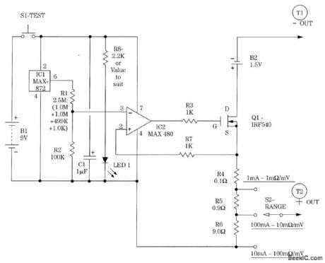
The figure shows the circuit of the milliohm adapter. It can apply 1A, 100 mA, or 10 mA to the resistance under test. The current application will indicate the resistance directly in millivolts if your voltmeter is set on the 2-V range. B1 is the high-current source, an alkaline battery capable of generating the 1 A used in the circuit's highest-current application mode. This must be an alkaline battery. A three-position switch enables user selection of the desired applied current to the DUT. S1 performs as a dual-function on/off switch. When a measurement is to be made, pressing S1 turns on the circuit, which consists of a micropower voltage reference chip IC1 and an op amp, IC2. 101's out-put is 2.500 V, and that voltage is divided by R1 and R2, producing 0.1Vat the input of IC2. This turns on Q1, creating a 0.1-V potential at its source terminal. The resistive divider (R4, R5, and R6) forms a current source along with Q1, the 1.5-V battery and the DUT's resistance. That is applied to the DUT through the two output terminals, T1 and T2. When you connect your voltmeter across these terminals, you can directly read the resistance of the DUT. An optional LED shows when the circuit is in test mode. The 1-A range of the instrument will drain the 1.5-V alkaline battery faster than the 9-V battery, so it is advisable for reasons of economy not to keep S1 depressed for protracted periods on that range, or else the battery- life will suffer. Releasing S1 will halt the current source through Q1 and the associated circuit path, and thus will shut off the current flow from the 1.5-volt battery. The same effect will occur if you disconnect the test leads. (View)
View full Circuit Diagram | Comments | Reading(0)
AGC_FOR_ADF
Published:2009/7/16 2:54:00 Author:Jessie

Gives uniform receiver response over wide dynamic range of input signal levels. Output of third i-f stage Q2 is applied across agc diode D1.-P. V. Sparks, Servo Filter and Gain Control Improve Automatic Direction Finder, Electronics,34:23, p 110-113. (View)
View full Circuit Diagram | Comments | Reading(649)
02_20000_Hz_VOLTAGE_CONTROLLED_RAMP
Published:2009/7/13 6:11:00 Author:May

With values shown, frequency of ramp can be varied over range of about 20 kHz by changing DC input voltage. Lowest frequency is set by R1. Adjust R2 to make average output 0V, and set desired output level with R3. Uses 555 IC timer as astable MVBR, with charge current being supplied by transistor. Voltage/frequency relationship is logarithmic, making oscillator suitable for use in sound synthesizers.-J. L. Brice, Voltage-Controlled Ramp Generator, Wireless World, June 1976, p 72. (View)
View full Circuit Diagram | Comments | Reading(879)
CRYSTAL_CONTROLLED_SUPERREGENERATIVE
Published:2009/7/16 2:54:00 Author:Jessie

Two high-frequency transistors connected as 20-kHz MVBR provide switching action at same rate for RF oscillations generated in crystal feedback path. Received AM signal induced in tank circuit of C1 will modulate exact switching point of circuit at rate directly proportional to modulation component of received signal. Choose L1, C1, and crystal for frequency desired. If at 10 MHz, standard WWV time broadcasts can be picked up. -I. Math, Math's Notes, CQ, Sept. 1972, p 36-37.
(View)
View full Circuit Diagram | Comments | Reading(2221)
AGC_WITH_VARICAP
Published:2009/7/16 2:53:00 Author:Jessie


Basic voltage-controlled capacitor circuit uses capacitance variation with voltage of back-biased diode constructed to have large capacitance changes, such as Varicap. Circuits give different insertion losses and gain changes. Left: 5 db insertion loss and 16 db gain control range for agc bias of 15 v. Center: 2 db loss and 11 db gain range. Right: 7 db loss and 18 db gain range. AII can be reasonably flat for 200-Mc bandwidth.-W. A. Rheinfelder, Designing Automatic Gain Control Systems, EEE, 13;1, p 53-57. (View)
View full Circuit Diagram | Comments | Reading(662)
| Pages:690/2234 At 20681682683684685686687688689690691692693694695696697698699700Under 20 |
Circuit Categories
power supply circuit
Amplifier Circuit
Basic Circuit
LED and Light Circuit
Sensor Circuit
Signal Processing
Electrical Equipment Circuit
Control Circuit
Remote Control Circuit
A/D-D/A Converter Circuit
Audio Circuit
Measuring and Test Circuit
Communication Circuit
Computer-Related Circuit
555 Circuit
Automotive Circuit
Repairing Circuit