
Circuit Diagram
Index 682
GAIING_WITH_VARICAPS_AND_TRIODES
Published:2009/7/16 2:10:00 Author:Jessie


Gives 100-db on-off ratio of 5.5-Mc signal, using small-amplitude positive-pulse gate (about 4 V) with two dual triodes and four tuned circuits with varicaps in each. Tuned circuits are shifted from parallel to series resonance by gating signal.-Gating with Varicaps, Electronic Circuit Design Hand-book, Mactier Pub. Corp., N.Y., 1965, p 211. (View)
View full Circuit Diagram | Comments | Reading(576)
AMPLIFIED_AGC_1
Published:2009/7/16 2:10:00 Author:Jessie

Uses d-c amplifier in agc circuit to keep output of communication receiver more nearly constant despite widely varying input signal. One drawback of amplified agc is that when d-c ampliler plate current drops, bias voltage at its cathode increases agc output and thereby reduces gain of controlled stages.-NBS, Handbook Preferred Circuits Navy Aeronautical Electronic Equipment, Vol. 1, Electron Tube Circuits, 1963, p N 12-4. (View)
View full Circuit Diagram | Comments | Reading(662)
SELF_SETIING_PULSE_PATTERN_GATE
Published:2009/7/16 2:09:00 Author:Jessie

Picks out pulses transmitted at fixed repetition frequency, in presence of random noise, to improve reliability of ionospheric pulse transmitter-receiver synchronizing link by factor of 50.-E. R. Schmerling, Self-Setting Servo Gate, Electronics, 31:3, p 71.
(View)
View full Circuit Diagram | Comments | Reading(498)
AMPLIFIED_AGC
Published:2009/7/16 2:08:00 Author:Jessie

Uses d-c amplifier in agc circuit to keep output of communication receiver more nearly constant despite widely varying input signal.-NBS, Handbook Preferred Circuits Navy Aeronautical Electronic Equipment, Vol. 1, Electron Tube Circuits, 1963, p N 12-4. (View)
View full Circuit Diagram | Comments | Reading(758)
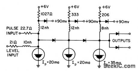
TUNNEL_DIODE_OR_GATE
Published:2009/7/16 2:08:00 Author:Jessie
Uses two cascaded monostables.- Transistor Manual, Seventh Edition, General Electric Co., 1964, p 370. (View)
View full Circuit Diagram | Comments | Reading(616)
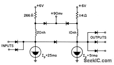
TUNNEL_DIODE_AND_GATE
Published:2009/7/16 2:05:00 Author:Jessie

Three cascaded monostables provide adequate gain for high-speed computer and logic.- Transistor Manual, Seventh Edition, General Electric Co., 1964, p 370. (View)
View full Circuit Diagram | Comments | Reading(996)
PREFERRED_VARIABLE_GATE_GENERATOR
Published:2009/7/16 2:04:00 Author:Jessie
Uses multivibrator to generate rectangular gate waveform whose duration is directly proportional to setting of potentiometer and is relatively independent of temperature effects. Used to produce movable markers for radar displays. Input signal is negative, from 10 to 20 V. Output is 12.5 V, with gate width adjustable from 10 to 10,000 microsec by changing values of R1 and C2.-NBS, Handbook Preferred Circuits Navy Aeronautical Electronic Equipment, Vol. II, Semiconductor Device Circuits, PSC 16 (originally PC 252), p 16-2. (View)
View full Circuit Diagram | Comments | Reading(515)
UNIJUNCTION_TRANSISTOR_GENERATES_DESIRED_NUMBER_OF_PULSES
Published:2009/7/16 2:04:00 Author:Jessie
Number of pulses generated each time switch St is operated increases linearly from 0 to 140 as battery voltage is increased from 11 to 35 v. Charge transferred from C1 to C2 fires transistor , discharging C2, with cycle repeating until C2 voltage drops below firing point.-R. Ferrie, Unijunction Circuit Generates Specific Number of Pulses, Electronics, 37:15, p 78. (View)
View full Circuit Diagram | Comments | Reading(717)
UJT_TRIGGERED_CROWBAR
Published:2009/7/13 21:25:00 Author:May
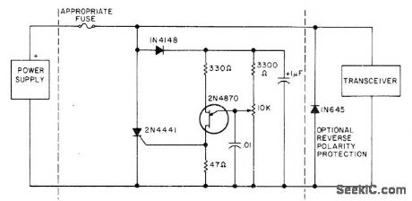
Circuit is used between transceiver and regulated 12-V power supply to protect transceiver from overvoltage or reverse polarity UJT permits precise setting of overvoltage level at which 2N4441 SCR crowbar operates. Fuse is blown within microseconds of overvoltage. Crowbar can be built into transceiver.-Circuits, 73Magazine, July 1977, p35. (View)
View full Circuit Diagram | Comments | Reading(1328)
SYNCHRONIZED_MAX038_FUNCTION_GENERATORS
Published:2009/7/13 21:24:00 Author:May
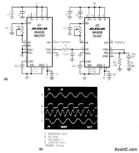
The MAX038's internal phase detector is intended primarily for use in phase-locked-loop (PLL) configurations. In (a), for example, the phase detector in IC2 enables that device to synchronize its operation with that of IC1. You connect the applied reference signal to IC2's TTL/CMOS-compatible phase-detector input (PDI) and connect the phase-detector output (PDO) to the input (FADJ) of the internal voltage-controlled oscillator. PDO is the output of an exclusive-OR gate-a mixer-which produces rectangular current waveforms at frequencies equal to the sum and difference of the PDI frequency and the MAX038 output frequency. These waveforms are integrated by CPD, to form a triangle-wave voltage output at PDO (b). The 10-Ω/100-pF pair at PDI limits that pin's rate of rise to 10 ns. (View)
View full Circuit Diagram | Comments | Reading(2155)
FAST_TUNNEL_DIODE_GATE
Published:2009/7/16 2:03:00 Author:Jessie
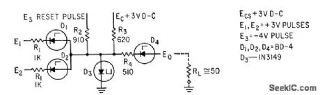
At coincidence between sampling pulse at one input and 100-Mc block pulse at other input, 11 ma current through D3 switches D3 to high level, making D4 pass current to load.-A. A. Fleischer and E. Johnson, New Digital Conversion Method Provides Nanosecond Resolution, Electronics, 36:18, p 55-57. (View)
View full Circuit Diagram | Comments | Reading(544)
CERAMIC_FILTER_DRIVE
Published:2009/7/13 21:22:00 Author:May

National LM3011 gain block provides three differential stages and current-source output suitable for driving 300-ohn,ceramic filter in IF amplifier of FM receivel,Circuit provides 60 dB of power gain to matched load.-''Audio Handbook,''National Semiconductor,Santa Clara,CA,1977,p 3-11-3-12. (View)
View full Circuit Diagram | Comments | Reading(717)
MECHANICAL_COUNTER_SPEEDUP
Published:2009/7/13 21:22:00 Author:May
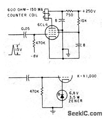
Vacuum-tube circuit doubles speed of counter, with minimum of overheating and other damage to counter coil and mechanism. Operation depends on pulsed overvolting for a limited time, along with some sliding overvolting wherein excess voltage is applied to coil when circuit is first completed, then reduced so it drops below normal operating voltage during pull-in time.-R. L. Ives, Circuit Modifications for Boosting Counter Speed, Electronics, 33:7, p112-114. (View)
View full Circuit Diagram | Comments | Reading(571)
TUNNEL_DIODE_PULSER
Published:2009/7/16 2:03:00 Author:Jessie

Switching voltage change of tunnel diode is differentiated and amplifed by grounded-base amplifer. With 8-V supply, 5-V output pulses are obtained into 91 ohms at clock rates up to 140 Mc.-M. V. Harrison and R. S. Foote, Tunnel Diodes Increase Digital-Circuit Switching Speeds, Electronics, 34:32 p154-156. (View)
View full Circuit Diagram | Comments | Reading(1054)
TRIAC_DRIVE
Published:2009/7/13 21:20:00 Author:May
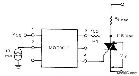
Motorola MOC3011 optoisolatoR serves as interface between 10-mA input circuit and gate of triac controlling AC load. Choice of triac depends on load being handled. Optoisolator detector chip responds to infrared LED; once triggered on, optoisolator stays on until input current drops below holding value of about 100μA.-P. O'Neil, Applications of the MOC3011 Triac Driver, Motorola, Phoenix, AZ, 1978, AN-780, p 2. (View)
View full Circuit Diagram | Comments | Reading(2650)
BASIC_PNP_GATE
Published:2009/7/16 2:02:00 Author:Jessie
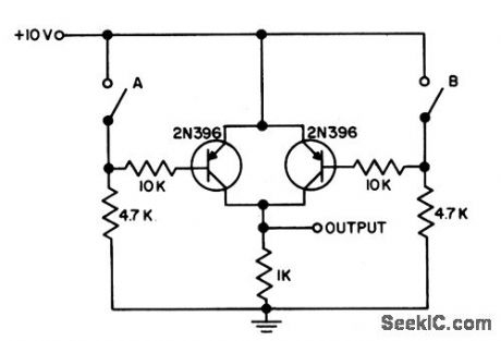
Circuit is and gate if closing of switch is an input, Circuit is or gate if opening of switch is an input. Provides phase inversion of input without complicating overall circuitry.- Transistor Manual, Seventh Edition, General Electric Co., 1964, p 176. (View)
View full Circuit Diagram | Comments | Reading(648)
VOX__FOR_SSB
Published:2009/7/13 21:20:00 Author:May
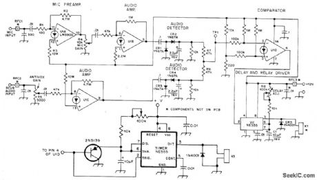
Uses LM3900 quad Norton opamp and NE555 timer operating from single supply. U1A and U1B amplify microphone signal. U1C amplifies audio sample obtained from station loudspeaker. Outputs of both amplifiers are converted to varying DC voltages by rectifiers in detector stages. Rectifier outputs are summed resistively by R6 and R7 for application to inverting input of voltage comparator U1D. Positive microphone signal drives comparator output low and triggers NE555, which in turn energizes 12-V relay K1 after delay set at about 10 ms by R8 to avoid losing first syllable. Same delay applies to relay dropout, to hold relay closed between words. If K1 drops out for fraction of second at end of timing cycle even though audio is present, add 2N5139 transistor to NE555 input as shown.-D. A. Blakeslee, A VOX for a Very Small Box, QST, March 1976, p 24-26. (View)
View full Circuit Diagram | Comments | Reading(1065)
PULSE_HEIGHT_TO_WIDTH_CONVERTER
Published:2009/7/16 2:02:00 Author:Jessie

Converts 0 to 2-V pulse to gate for pulse height to pulse width conversion. Gate width, directly proportional to data pulse amplitude, is applied to dock circuits.-W. W. Grannemann et al., Pulse-Height-to-Digital Signal Converter, Electronics, 33:2, p 58-60. (View)
View full Circuit Diagram | Comments | Reading(1270)
BILATERAL_AMPLIFIER
Published:2009/7/13 21:19:00 Author:May
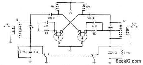
When switch is in position shown, signal entering through T1 is amplified by first transistor and fed from its drain terminal to output through resonant transformer T2. Second transistor is not operational because it now has cutoff bias between gate and source. When switch position is reversed, incoming signal is applied to transistor at right through T2 and removed from left side of circuit to give changeover in signal direction. First transistor is inactive now.-E. M. Noll, FET Principles, Experiments, and Projects, Howard W. Sams, Indianapolis, IN, 2nd Ed., 1975, p 198-199. (View)
View full Circuit Diagram | Comments | Reading(703)
GATED_MVBR
Published:2009/7/16 2:01:00 Author:Jessie
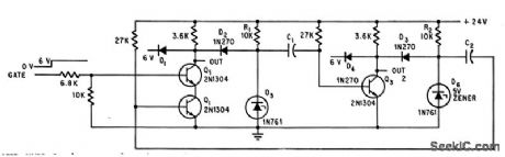
Complementary pulse trains appear at outputs 1 and 2 when gate is applied.-R. Newmeyer, Gated Multivibrator Output Provides Constant Pulse Width, Electronics, 38:26, p 69. (View)
View full Circuit Diagram | Comments | Reading(613)
| Pages:682/2234 At 20681682683684685686687688689690691692693694695696697698699700Under 20 |
Circuit Categories
power supply circuit
Amplifier Circuit
Basic Circuit
LED and Light Circuit
Sensor Circuit
Signal Processing
Electrical Equipment Circuit
Control Circuit
Remote Control Circuit
A/D-D/A Converter Circuit
Audio Circuit
Measuring and Test Circuit
Communication Circuit
Computer-Related Circuit
555 Circuit
Automotive Circuit
Repairing Circuit