
Circuit Diagram
Index 698
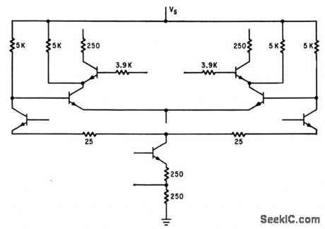
TWO_STAGE_OPERATIONAL_AMPLIFIER
Published:2009/7/16 3:48:00 Author:Jessie


Maximum gain at room temperature is 36,000.Emitter-follower output stages are used with zener diodes to shift d-c level. Input stage uses Darlington inputs. Input impedance is above 1 meg. Frequency rolloff of 6 db/octave begins at 50 kc.-C. L. Heizman and D. G. Peterson, Circuit Analysis: A Monolithic Integrated Operational Amplifier, EEE, 13:5, p 80-84. (View)
View full Circuit Diagram | Comments | Reading(793)
10_40_METERS_TO_35_4_MHz
Published:2009/7/16 3:48:00 Author:Jessie

Five-band converter is designed for use with miniaturized communication receiver tuning from 3.5 to 4 MHz Signals for 80-meter band are fed directly to receiver. Two-gang tuning capacitor used to peak converter front end is film-dielectric type taken from transistor FM radio. -R. Megirian, Design Ideas for Miniature Communications Receivers, Ham Radio, April 1976, p 18-25. (View)
View full Circuit Diagram | Comments | Reading(1698)
2_AND_4_INPUT_IVOR_GATE
Published:2009/7/16 3:48:00 Author:Jessie

Performs general-purpose and, or, and inversion functions in compatible set of digital logic circuits for computer, control and communication equipment. Can be used as and gate for positive levels or positive-going pulses, as or gate for negative levels or negative-going pulses, and as inverter for both levels and pulses.-NBS, Handbook Preferred Circuits Navy Aeronautical Electronic Equipment, Vol. II, Semiconductor Device Circuits, PSC 7 (originally PC 210), p 7-2. (View)
View full Circuit Diagram | Comments | Reading(640)
LOGIC_CONTROLS_25_W_LAMP
Published:2009/7/13 4:44:00 Author:May

Ordinary 1-A bridge is used with H74C1 optoisolatorto pass full current to 25-W lamp when logic inρut goes low (to around,so full 5 V is applied to light source in optoisolator).-D. D. Mickle, Practical Computer Projects, 73 Magazine, Jan. 1978, p 92-93. (View)
View full Circuit Diagram | Comments | Reading(761)
BICOLOR_LED_SPST_SWITCH
Published:2009/7/13 4:43:00 Author:May

A transistor and a few resistors control two LEDs where the cathodes have a common lead. (View)
View full Circuit Diagram | Comments | Reading(1193)
HIGH_VOLTAGE_PULSE_GENERATOR
Published:2009/7/16 3:48:00 Author:Jessie

Square-wave input to transistor Q1 triggers scr on and off, inducing high-voltage damped-oscillation pulse in secondary of T1. Used for auto ignition and other applications requiring up to 30 kv from 0 to 400 times per second. -D. R. Grafham, Now the Gate Turnoff Switch Speeds Up D-C Switching, Electronics, 37:12, p 64-71. (View)
View full Circuit Diagram | Comments | Reading(3173)
LARGEST_SIGNAL_SELECTOR
Published:2009/7/16 3:48:00 Author:Jessie

Selects single channel that has greatest amplitude, using single nor-like transistor circuit per channel-Base mixer resistance network establishes signal bias level at greatest signal level en countered in all except designated chancel-Channel transistor then conducts only when its signal at emitter is greater than all other signals.-L. R. Brown, Nonscanning Character Reader Uses Coded Wafer, Electronics, 33:48, p 115-117. (View)
View full Circuit Diagram | Comments | Reading(649)
CROSS_CONNECTED_INVERTERS_AS_FLIP_FLOP
Published:2009/7/16 3:48:00 Author:Jessie

Output levels are 0 and 3.5 V. Switching times ore 20 to 34 nsec for resistive loads and 30 to 44 nsec for capacitive loads.-W. D. Roehr, For Computers...Basic RCTL Circuits, Motorola Application Note AN-129, Nov, 1965. (View)
View full Circuit Diagram | Comments | Reading(572)
CLOCK_PULSES
Published:2009/7/16 3:48:00 Author:Jessie

Tunnel-diode one-shot produces number of pulses in series, proportional to value of L1 and width of input pulse.-C. A. Budde, Pulse Width Converted to Pulse Sequence, Electronics, 38:4, p 86-87. (View)
View full Circuit Diagram | Comments | Reading(651)
AUDIO_AMPLIFIER
Published:2009/7/16 3:47:00 Author:Jessie

Uses Mitsubishi chromium-silicon and nickel-chromium thin-film resistors in hybrid arrangement with conventional transistors.-Y. Tarui, Japan Seeks Its Own Route to Improved IC Techniques, Electronics, 38:25, p 90-98. (View)
View full Circuit Diagram | Comments | Reading(0)
UP_DOWN
Published:2009/7/16 3:47:00 Author:Jessie

Circuit shown was developed for use in 5645.8-kHz IF amplifier of Drake R-4B amateur-band receiver, to utilize high-performance characteristics of Sherwood Engineering CF-125/8 CW crystal filter having bandwidth of only 125 Hz. Texas Instruments TL442 double-balanced mixers convert IF signal to 5695-kHz center frequency of filter and convert filter output back to IF value. Same crystal oscillator serves for both upconversion and downconversion. Gives true single-signal reception. Article covets procedures for interfacing any crystal filter with any receiver IF value. -H. Sartori, An Up/Down Filter Converter, Ham Radio, Dee. 1977, p 20-25. (View)
View full Circuit Diagram | Comments | Reading(1941)
RECEPTOR_TYPE_NEURON_MODEL
Published:2009/7/16 3:47:00 Author:Jessie

Uses integrator quench circuit. Outputs of 100 or more such neuron circuits are combined so experiments can be repeated consistently,with minimal interaction.-C. M. Wiley, Bionics on Program at Midwest's NEC, Electronics, 34:40, p 61-67. (View)
View full Circuit Diagram | Comments | Reading(621)
INTEGRATED_p_MOST_BROADBAND_AMPLIFIER
Published:2009/7/16 3:47:00 Author:Jessie

Hole-conducting metal-oxide semiconductor transistor (p-most) and metal-oxide semiconductor capacitor give gain of 5 down to a few cps for integrated stage.-F. M., Wanlass, Novel Field-Effect Device Provides Broadband Gain, Electronics, 36:44, p 30-33. (View)
View full Circuit Diagram | Comments | Reading(495)
TWO_STROBE_SENSE_AMPLIFIER
Published:2009/7/16 3:46:00 Author:Jessie
Seven-transistor sense amplifier on single 61 by 70-mil silicon chip has overall gain of 200.-M. F. Wolff, Computer in the Microcircuit Design Room, Electronics, 37:12, p 100-104. (View)
View full Circuit Diagram | Comments | Reading(506)
X_AMPLIFIER_FOR_COINCIDENT_FLUX_MEM_ORY
Published:2009/7/16 3:46:00 Author:Jessie

Inputs to and gate are dock read or write pulse and first two binary digits of horizontal address, forming one of the two translations for horizontal matrix of 1,120-bit memory.-H. F. Priebe, Jr., Three-Hole Cores for Coincident-Flux Memory, Electronics, 33:31, p 94-97. (View)
View full Circuit Diagram | Comments | Reading(500)
PRESSUE_CONTROLLED
Published:2009/7/16 3:46:00 Author:Jessie

Frequency of avalanche oscillator in integrated circuit using RC103 transistors varies linearly from 100 to 124 kc as stylus pressure on transistor Q2 is increased from zero to 7 grams -R. C. Wonson, Stress-Sensitive Integrated Circuits, Electronics, 38:14, p 81-84. (View)
View full Circuit Diagram | Comments | Reading(497)
400000_RPM_TACHOMETER_DISPLAY
Published:2009/7/16 3:46:00 Author:Jessie
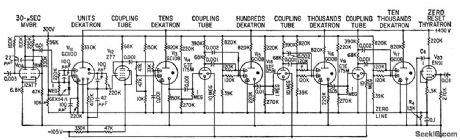
Has five Dekatron tubes arranged in cascade. Negative-going pulses from plate of gating tube are fed to 30-microsec one-shot mvbr V 10. Tetrode thyratron returns Dekatron to zero at end of counting period.-J. K. Goodwin, Digital Tachometer Aids in Turbine Design, Electronics, 32:15, p 58-61. (View)
View full Circuit Diagram | Comments | Reading(617)
MULTIPURPOSE_CHIP
Published:2009/7/16 3:45:00 Author:Jessie

Monolithic chip con sisting of six resistors and two identical transistors serves three different functions in f-m receiver. Two transistors permit cascade amplifier configuration, giving low noise fig ure and good power gain ct high frequencies.-R. L. Sanquini, Multipurpose Chips Cut Costs of F-m Receiver, Electronics, 39:10, p 80-82. (View)
View full Circuit Diagram | Comments | Reading(487)
VOICE_AMPLIFIER
Published:2009/7/16 3:45:00 Author:Jessie
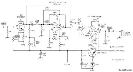
Includes audio preamp, RC active filter, audio output stage, and voltage regulator, operating from 12.5-V supply rated 300mA or more. Developed as low-distortion audio amplifier for communication receiver.Two taps for regulated supply provide regulated 8.5 V at 250 mA for other circuits. With filter out, changing input frequency from 300 to 3000 Hz has little effect on output. Switching in audio filter should attenuate all frequencies not in 700-Hz passband of filter. Gain is adjustable over wide range. Output will drive small loudspeaker of 4-16 ohms or headphones of 4-2000 ohms. Can also be used as test bench audio amplifier, intercom, or with code-practice oscillator. -J. Rusgrove, A General-Purpose Audio Amplifier, QST, Nov. 1976, p 32-34. (View)
View full Circuit Diagram | Comments | Reading(2286)
TRANSISTOR_DECREASES_RESET_TIME
Published:2009/7/16 3:45:00 Author:Jessie
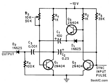
Time for recharging C1 is reduced by factor of 30 when Q3 is added to conventional astable mvbr.-S. A. Bell, Added Transistor Decreases Multivibrator Reset Time, Electronics, 37:21, p 72-73. (View)
View full Circuit Diagram | Comments | Reading(648)
| Pages:698/2234 At 20681682683684685686687688689690691692693694695696697698699700Under 20 |
Circuit Categories
power supply circuit
Amplifier Circuit
Basic Circuit
LED and Light Circuit
Sensor Circuit
Signal Processing
Electrical Equipment Circuit
Control Circuit
Remote Control Circuit
A/D-D/A Converter Circuit
Audio Circuit
Measuring and Test Circuit
Communication Circuit
Computer-Related Circuit
555 Circuit
Automotive Circuit
Repairing Circuit