
Circuit Diagram
Index 695
AUTOMOTIVE_NEON_DRIVER
Published:2009/7/13 5:09:00 Author:May

A 555 timer drives driver transistor Q1 and switching transistor Q2 at 25 to 30 kHz. T1 is wound on a ferrite core (try using a core from an old B/W TV flyback) and has the windings arranged as shown in the schematic. About 2500 Vac p-p is produced, so be careful to avoid any possibility of contact with this voltage, as it can cause a bad shock or RE burn. The neon tube is a custom-size item that can be made up at any neon sign shop or possibly purchased commercially. It is not legal to illuminate certain parts of your vehicle in some parts of the United States and in some nations. (View)
View full Circuit Diagram | Comments | Reading(1930)
TRANSDUCER_DRIVEN_CRYSTAL_OSCILLATOR
Published:2009/7/13 5:07:00 Author:May

Sensitive 70-Mc one-tube oscillator feeds local and remote tank circuits to which capacitive or inductive transducers may be connetted, for conversion of displacement, temperature, pressure, and other variables to corresponding changes in d-c output voltage.Will give up to 250V change per micromicro-farad of transducer capacitance change.-L. J.Rogers, Sensitive Transducers Use One-Tube Crystal Oscillator, Electronics, 32:40, p48-49. (View)
View full Circuit Diagram | Comments | Reading(1293)
RADIO_AUTOMATIC_LEVEL_CONTROL
Published:2009/7/13 5:06:00 Author:May

This experimental circuit automatically increases the volume of a car radio when the vehicle's speed (and consequently road and wind noise) rises, and retums the volume to a pleasant level at lower speeds. This relieves the driver of the distracting chore of continually fiddling with the radio's volume control. In the figure, a special tachometer IC type LM2917 takes its input from the ignition system's contact bre.aker points and converts this into a voltage that is directly proportional to engine speed. This voltage will always be in the range of 0 to 5 V anct is used to illuminate a miniature filament lamp LP1. On either side of this lamp is mounted a pair of light-dependent resistors (LDRs) that are connected in series with the wipers of the radio's volume control potentiometers. A ganged potentiometer across each of the LDRs sets the minimum volume level, the radio's own volume being used for the high level. The value of capacitor C2 determines the range over which the unit will function satisfactorily. A suggested value of 4n 7 would be a suitable starting point for further experimentation. The 100-kΩ input resistor (R1) should be placed as near as possible to the ignition coil to prevent RFI (radio frequency interference) and to ensure that the contact breakers are not shorted out should the wire short to earth (chassis) for any reason. (View)
View full Circuit Diagram | Comments | Reading(770)
HIGH_COMPLIANCE_CURRENT_SOURCE
Published:2009/7/13 5:05:00 Author:May

Non-inverting input of LM143 high-voltage opamp senses current through R4 to establish output current that is proportional to input voltage. With ±38 V supply, compliance of current source is ±28V. - Linear Applications, Vol. 2, National Semiconductor, Santa Clara, CA,1976, AN-127,p3. (View)
View full Circuit Diagram | Comments | Reading(931)
LOGIC_DRIVE_FOR_INDUCTIVE_LOAD
Published:2009/7/13 5:04:00 Author:May

When output of NAND gate goes high and furnishes 10 mA to LED of Motorola M0C3011 optically coupled triac driver, output of optoisolator provides necessary trigger for triac controlling inductive load.C1 is 0.22 μF for load power factor of 0.75 and 0.33 μF for 0.5 power factor. Omit C1 for resistive load. R1, R2, and C1 serve as snubber that limits rate of rise in voltage applied to triac.-P. O'Neil, Applications of the MOC3011 Triac Driver, Motorola, Phoenix, AZ, 1978, AN-780 p 2. (View)
View full Circuit Diagram | Comments | Reading(1096)
4_20_mA_SOURCE
Published:2009/7/13 5:04:00 Author:May

DigitaI input to multiplying digital-to-analog converter determines load current in range of 4 to 20 mA with 15.6-μA resolution. R1 adjusts ratio of full-scale to zero-scale current at output 1 of MDAC and R3 sets circuit offset and span to give correct end-range currents for load. Maximum load compliance is 25 V. Opamp types are not criticaL-J. Wilson and J. Whitmore, MDAC's Open Up a New World of Digital-Control Applications, EDN Magazine, Sept. 20, 1978, p 97-105. (View)
View full Circuit Diagram | Comments | Reading(1414)
20_mA_FLOATING_SOURCE
Published:2009/7/13 5:03:00 Author:May

Battery-operate d circuit shown gives adequate stability for strain-gage bridge. Uses four alkaline penlight cells to provide ±3 V for 741 opamp. E1 is chosen to give adequate voltage for intended load at maximum load current. Temperature stability is 0.7 μA/℃ from 0 to 50℃. -R. Tenny, Isolated Current Source, EDN Magazine, April 20, 1973, p 85. (View)
View full Circuit Diagram | Comments | Reading(810)
450_MC_TO_105_MC_WITH_2N2996
Published:2009/7/13 5:02:00 Author:May


Local Colpitts oscillator operates at 345 Mc; it can deliver 5mw, but only 1 mw is required by oscillator-stabilizing buffer for good mixing action. R-f stage ahead of converter provides power gain of 13 db at noise figure of only 5.9 db.-Texas Instruments Inc. Solid-State Communications, McGraw-Hill, N.Y.1966, p305. (View)
View full Circuit Diagram | Comments | Reading(629)
DAYTIME_RUNNING_LIGHT_CIRCUIT
Published:2009/7/13 5:02:00 Author:May

The DRL circuit is a variable-duty-cycle power oscillator that allows pulses of current to be applied to the headlights whenever the ignition of the vehicle is turned on. The 12-Vdc power that drives the circuit is taken from two sources in the vehicle. Power for the headlights is provided by the vehicular battery and generator system, and is input through fuse F1 to the circuit. The power source for the digital or logic part of the circuit is the + 12-V line that feeds the ignition system of the vehicle. When the ignition is turned on, the circuit is on, and when the ignition is turned off, so is the circuit. When the ignition is on, power is applied through D1 to operate IC1, a 555 timer that is connected as a free-running multivibrator. Pin 3 of IC1 provides the output of the oscillator; the duty cycle is determined by the following ratio:
(R1 + R2) /R3
Potentiometer R1 allows the duty cycle of the negative part of the waveform to be adjusted from about 10 percent to almost 50 percent. Adjustment capability is provided so that the intensity of illumination can be set as desired. A set of logic gates (IC2), powered by the battery and generator, is used to control the operation of the circuit. When the ignition is off, the logic output of pin 3 of IC2-a is high. Under that high-logic condition, the transistors are not forward-biased and the headlights remain off. When the ignition is on, the oscillator is powered through D1. The pulse train output of IC1 appears simultaneously at the gates of Q1 and Q2. Those two transistors then feed + 12-V pulses through their respective diodes, D3 and D4, to the low-beam headlights of the vehicle. The diodes provide isolation between the DRL circuit and the electrical system of the vehicle. The design of the circuit makes it possible to add second pairs of hex-FET transistors and corresponding diodes to the circuit and have them driven by IC2-c. Thus, if desired, the taillights of the vehicle may also be used for DRL operation. (View)
View full Circuit Diagram | Comments | Reading(5092)
SIMPLE_CONTINUITY_TESTER
Published:2009/7/16 2:38:00 Author:Jessie

This figure shows the circuit for a simple, but safe, continuity tester. (View)
View full Circuit Diagram | Comments | Reading(0)
CONSTANT_WIDTH_HIGH_CURRENT_PULSES
Published:2009/7/16 2:37:00 Author:Jessie

Circuit generates negative pulses from -2 to -12 v with rise and fall limes less than 30 nsec. Amplitude and spacing depend on supply voltage. For positive output pulses, use npn transistors and positive supply.- C. P. Hohberger, Fast Pulse Generator Tests Digital Circuit Delay, Electronics, 39:4, p 88-89.
(View)
View full Circuit Diagram | Comments | Reading(583)
LOGIC_TRIGGERED_TRIAC
Published:2009/7/13 5:02:00 Author:May

Pulsed output from microprocessor controls gate drive of triac through SN7475 clock and transistor. Pulse from one output port of microprocessor is applied to D input of clock simultaneously with pulse from communications register unit (CRU) going to clock input, to raise Q output of clock to logic 1. Output remains high until another pulse from CRU returns it to zero, thus giving latching action. High output turns on transistor and supplies about l00-mA gate drive to TlC263 25-A triac.- Thyristor Gating for μP Applications, Texas Instruments, Dallas, TX, 1977, CA-191,p4. (View)
View full Circuit Diagram | Comments | Reading(1976)
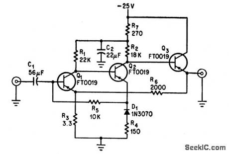
LOW_NOISE_LOW_LEVEL_AUDIO_AGC
Published:2009/7/16 2:37:00 Author:Jessie

Q1 and Q2 are active amplifier elements.Agc range is 60 db, maximum output signal is 1 v, and maximum input signal is 2 mv. Noise figure is 6 db. Agc circuit here uses shunting diode D1.-Texas Instruments Inc., Transistor Circuit Design, McGraw-Hill, N.Y., 1963, p 179. (View)
View full Circuit Diagram | Comments | Reading(2007)
LOW_OUTPUT_IMPEDANCE_I_F
Published:2009/7/16 2:36:00 Author:Jessie
Can provide impedances as low as 2 ohms and low noise figure, to take advantage of superior noise performance of backward diodes as mixers and detectors while overcoming their very low impedance at intermediate frequencies in range from 1 kc to 100 kc. Used in continuous-wave doppler radar systems.-R. O. Wright, New Twist for Backward Diode: Help from Low-Noise Amplifier, Electronics, 39:14, p 74-77. (View)
View full Circuit Diagram | Comments | Reading(643)
SQUARE_WAVE_TUNNEL_DIODE
Published:2009/7/16 2:36:00 Author:Jessie

Short-circuited coaxial cable may be connected either in series or in parallel with tunnel diode of basic relaxation oscillator,to get square-wave output with excellent frequency stability over entire bias range.-Wen-Hsiung Ko, Designing Tunnel Diode Oscillators, Electronics, 34:6, p 68-72. (View)
View full Circuit Diagram | Comments | Reading(991)
TRANSISTOR_AS_ATTENUATOR
Published:2009/7/16 2:35:00 Author:Jessie

Servo-type agc for transistor receivers holds audio output constant despite changes in r-f input. Wideband low-noise amplifier is used in transmission loop, while direct-coupled grounded-emitter amplifier drives detector circuit in feedback loop.-F. Susi, Solving the AGC Di-lemma-Servo System Uses Attenuator, Electronics, 36:29, p 60-62. (View)
View full Circuit Diagram | Comments | Reading(970)
I_F_WITH_LOW_PASS_FILTER
Published:2009/7/16 2:35:00 Author:Jessie
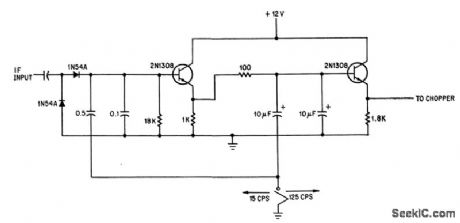
Cutoff frequency of signal-channel amplifier for frequency-measuring spectrum analyzer is 15 cps with RC fiber as shown and 125 cps when switch grounds lowest filter lead.-C. W. Wilson, Phase-Locked Marker Improves Spectrum Analyzer's Accuracy, Electronics, 39:3, p 88-92. (View)
View full Circuit Diagram | Comments | Reading(691)
SINGLE_PULSE
Published:2009/7/16 2:35:00 Author:Jessie
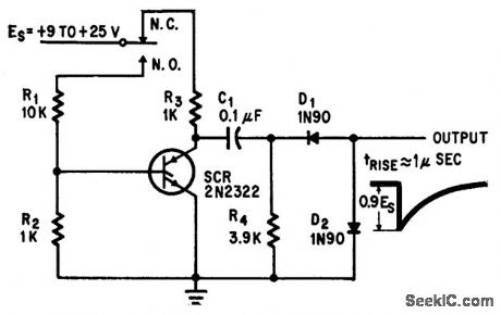
Push button fires scr to produce single pulse with rise time of 1 micro. sec.-R. W. Bailey, Push Button SCR Equals Fast Pulse, Electronics, 37:30, p 41-42. (View)
View full Circuit Diagram | Comments | Reading(742)
CONTINUITY_CHECKER
Published:2009/7/16 2:35:00 Author:Jessie

The checker is built around a 4N35 optocoupler. When the test leads are shorted by a resistance, it turns IC1 on by pulling pins 2 and 4 low, allowing current to flow through pins 6 and 5. The current to pin 5 flows through either the buzzer or the LED, depending on the position of S1. To test continuity of 50Ω or less, use the buzzer as the indicator. For continuity of up to 1000Ω, use the LED. The circuit can also be used to check PN junctions of transistors and diodes, with less possibility of damaging such sensitive components. For that, use the LED, and connect the lead from pin 2 of IC1 to the P side. The supply can be from 7.5 to 9V. To catch fast pulses, trigger a monostable with pin 5, and use it to drive the LED and the buzzer. The monostable will act like a pulse stretcher. (View)
View full Circuit Diagram | Comments | Reading(0)
THIN_FILM_LOG_I_F_AMPLIFIER
Published:2009/7/16 2:34:00 Author:Jessie

Translation ampliter limits bandwidth at input, while video emitter-follower matches 10-v output to load. All seven log i-f stages use thin-film circuits.-R. Leslie and T. Townsend, Inductors No Problem: New Thin-film Amplifier, Electronics, 36:23, p 46-49. (View)
View full Circuit Diagram | Comments | Reading(572)
| Pages:695/2234 At 20681682683684685686687688689690691692693694695696697698699700Under 20 |
Circuit Categories
power supply circuit
Amplifier Circuit
Basic Circuit
LED and Light Circuit
Sensor Circuit
Signal Processing
Electrical Equipment Circuit
Control Circuit
Remote Control Circuit
A/D-D/A Converter Circuit
Audio Circuit
Measuring and Test Circuit
Communication Circuit
Computer-Related Circuit
555 Circuit
Automotive Circuit
Repairing Circuit