
Circuit Diagram
Index 684
5_AND±12_V_ac_POWERED_SWITCHING_SUPPLY
Published:2009/7/16 1:54:00 Author:Jessie

This supply uses an SGS-Thomson UC3842 IC in an off-line flyback regulator, providing + 5 V at 4 A and± 12 V at 300 mA. This enables a small high-frequency (50 kHz) transformer, to handle large amounts of power that are normally handed by a 60-Hz transformer. Q1 is a 5-A 500-V MOSFET, and the diodes are fast-recovery types. T1 has a 45-turn primary winding of #26 wire. The 12-V windings are each 9 turns of #30 wire, bifilar wound. The 5-V winding is 4 turns of four bifilar #26 wires. The control (feed-back) winding is two bifilar, parallel10-turn, #30 windings. The core is Ferroxcube EC35-3C8 with a 3/8 center leg. (View)
View full Circuit Diagram | Comments | Reading(6733)
COLD_CATHODE_FLUORESCENT_LAMP_DRIVER
Published:2009/7/13 20:55:00 Author:May

In this circuit, the lamp is driven sinusoidally, minimizing RF emissions in sensitive portable applications. Lamp intensity is controlled smoothly from zero to full brightness with no hysteresis or pop on. This floating bulb circuit configuration extends the illumination range for the bulb because parasitic bulb-to-display-frame capacitive losses are minimized. The feedback signal is generated by monitoring the primary-side Royer converter current between the BAT and Royer pins. The LT1184F current-mode switching regulator and L2 provide an average current to Q1 and Q2, which form a Royer-class converter along with L1 and C1. The lamp is driven by L1's secondary. Feedback to the LT1184F is provided on the primary side of L1 for floating bulb configurations, whereas feedback in the grounded configuration is provided by sensing one-half of the average bulb current. The oscillator frequency is 200 kHz, which minimizes the size of the required magnetics.
(View)
View full Circuit Diagram | Comments | Reading(1701)
ULTRASONIC_RECEIVER
Published:2009/7/16 1:54:00 Author:Jessie
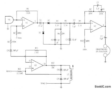
Amplifies output of 40-kHz ultrasonic transducer M1 by mixing in opamp A1 with signal of local oscillator A3 to produce AF signal for further amplification by A2 which drives headphones. Opamp sections are from Motorola MC3401P quad opamp. Diodes are 1N914 or equivalent, L1 is Miller 6315 4-30 mH Supply can be 9-12V,Transmitter can be wide-range audio amplifier capable of handling 38-42 kHz, driving similar ultrasonic transducer. -C. D. Rakes, Integrated Circuit Projects, ″ Howard W. Sams, Indianapolis, IN, 1975, p 26-29. (View)
View full Circuit Diagram | Comments | Reading(5661)
THYRISTOR_SWITCH
Published:2009/7/13 20:52:00 Author:May

When circuit of conventional P-gate thyristor is grounded by switch, negative-going pulse is applied to thyristor cathode, which reverse-biases the diode. When thyristor conducts, diode is forward-biased and has only about 0.7-V drop. Use low-voltage diode, rated for full load current. Opening of relay contacts makes circuit switch off.-R. V. Hartopp, Grounded Gate Thyristor, Wireless World, Feb. 1977, p 45.
(View)
View full Circuit Diagram | Comments | Reading(1026)
ENHANCED_TUNNEL_DIODE_NOR_CIRCUIT
Published:2009/7/16 1:54:00 Author:Jessie

Clock pulse through D2 triggers tunnel diode to its high voltage state to produce an output only when there are no inputs. Hybrid circuit will operate above 100 Mc, ct high fan-in and fan-out, and uses low-cost parts.-P. Chow and J. Cubert, A Key to Nanosecond Switching, Electronics, 36:42, p 42-45. (View)
View full Circuit Diagram | Comments | Reading(668)
SPEED_TRIPLING_COUNTER_DRIVE
Published:2009/7/13 20:51:00 Author:May
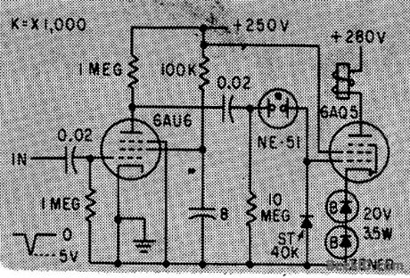
Increased speed of 25-cps electromechanical counter to 75 cps without affecting accuracy of count.Circuit circuit arrangement simplifies power supply requirements. Zener diodes eliminate need for bias supply.-R.L.lves, Circuit Modifications for Boosting Counter Speed, Electronics, 33:7, p112-114. (View)
View full Circuit Diagram | Comments | Reading(816)
TUNNEL_DIODE_THIN_FILM_TOGGLING_CIR_CUIT
Published:2009/7/16 1:53:00 Author:Jessie

Supply biases flim-diode combination at constant 5 v at 25 ma so two stable diode voltages are about 0.05 and 0.4 v. This means that bias current through film winding will flow in either of two directions, depending on state of diode.-T. A. Smay and A. V.Pohm, Design of Logic Circuits Using Thin Films and Tunnel Diodes, Electronics, 34:35, p 59-61. (View)
View full Circuit Diagram | Comments | Reading(464)
2945_MHz_PREAMP
Published:2009/7/16 1:52:00 Author:Jessie

Reduces noise figure of average communication receiver 2.5 dB and adds up to 20 dB of gain, as required for reception of 29.45-MHz satellite beacon signals. Q1 is RCA 40673 or almost any other dual-gate MOS-FET, with shield partition across the device. L2 is 10 turns No. 24E spaced on 1/4-inch slug-tuned core, with 2 turns over cold end for L1. L3 is 10 turns No. 24E closewound on 1/4-inch slug-tuned core, with 2 turns over cold end for L4.-J. D. Colson, An Oscar Preamp That Works Wonders, 73 Magazine, July 1975, p 31-32. (View)
View full Circuit Diagram | Comments | Reading(2684)
OPTOISOLATOR_DRIVE_FOR_240_VAC_LOAD
Published:2009/7/13 20:50:00 Author:May

wo Motorola M0C3011 optically coupled triac drivers are used in series to overcome voltage limhation of single coupler when triggering triac connected to control 240-VAC load. Two 1-megohm resistors equalize voltage drops across couplers.-P.O'Neil, Applications of the MOC3011 Triac Driver, Motorola, Phoenix,AZ,1978,AN-780,p5. (View)
View full Circuit Diagram | Comments | Reading(856)
SENSE_AMPIJFIER
Published:2009/7/16 1:52:00 Author:Jessie

Minimum input required from cores of random-access memory is 30 mv, and minimum output pulse is 6 v. Amp lifier is balanced to reduce common-modenoise.-G. E. Lund and D. R. Faulis, Expandable Random Access Memories, Electronics, 33:11, p 164-166. (View)
View full Circuit Diagram | Comments | Reading(538)
TRIAC_FOR_INDUCTIVE_LOADS
Published:2009/7/13 20:48:00 Author:May

Simple triac gating circuit applies AC power to inductive load when low-power switch S1 is closed. R1 and C1 provide dv/dt suppression.-C. A. Farel and D. M. Fickle, Triac Gating Circuit, EDN/EEE Magazine, Jan. 1, 1972, p 72-73. (View)
View full Circuit Diagram | Comments | Reading(2522)
DIODE_GATE
Published:2009/7/16 1:52:00 Author:Jessie


Input signal from ring counter applies reverse bias through isolating transistor Q1 to diode gate and base of Q2, which then supplies current to common load of multichannel scope display.-J. E. Russell, Ten Signals at a Glance, Electronics, 37:19, p 54. (View)
View full Circuit Diagram | Comments | Reading(642)
400_Hz_TRIGGER_FOR_SCR
Published:2009/7/13 20:44:00 Author:May

Simple UJT oscillator combined with pulse transformer provides pulses required for firing 2N1764 SCR.Article gives design data for pulse transformer,along with design equations.-W. Dull, A, Kusko, and T. Knutrud, Pulse and Trigger Transformers-Performance Dictates Their Specs, EDN Magazine, Aug. 20, 1976, p 57-62. (View)
View full Circuit Diagram | Comments | Reading(1020)
POSITIVE_AND_NEGATIVE_VOLTAGE_SWITCHING_SUPPLY
Published:2009/7/16 1:51:00 Author:Jessie

The LT1172 is configured as a step-up converter. C2 is charged by L1 and discharges into C4 when the LT1172's power switch goes to ground. Resistor R3 adjusts the output voltage between -12 and -24 V. (View)
View full Circuit Diagram | Comments | Reading(1684)
VOLTAGE_SENSITIVE_SWITCH
Published:2009/7/13 20:42:00 Author:May

RCA 40527 triac is triggered by small neon. After breakdown occurs bidirectionally at 88 V, triac takes over as short-circuit. D1 can be any other voltage breakdown device, such as diac or zener, and thyristor can be used in place of triac to give unilateral switching. Applications include use as power crowbar, with breakdown level set by artificial resistance-controlled zener.-L. A. Rosenthal, Breakdown and Power Devices Form Unusual Power Switch, EDN Magazine, July 5, 1974,p74-75. (View)
View full Circuit Diagram | Comments | Reading(930)
DIGIT_LINE_DECOUPLER
Published:2009/7/16 1:51:00 Author:Jessie

Diode switch and biasing network disconnect sense amplifier, allowing common-mode signal of about 1 v to reach difference amplifier. This signal is almost completely rejected at output, so amplifier is ready for next cycle 0.5 microsec after end of rewriting.-A. Melmed, R. Shevlin, and W. Orvedahl, Diode Steering Increases Speed of Magnetic Memories, Electronics, 34:37, p 68-70. (View)
View full Circuit Diagram | Comments | Reading(521)
SIGNAL_BRIDGE_FET
Published:2009/7/16 1:51:00 Author:Jessie


Provides pulsed c-w output from 300- kc c-w input.On-off ratio is 50 db. Insertion loss is 15 db with 510-ohm output load. Requires no adjustment. Used in sonar experiments.-F. J. Murphree and J. Bealor, FET in Bridge Circuit Gates a 300-KC Signal, Electronics, 38:9, p 60-61. (View)
View full Circuit Diagram | Comments | Reading(550)
AMPLIFIER_DRIVER_SPEEDS_UP_COUNTER
Published:2009/7/13 20:41:00 Author:May
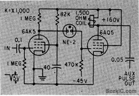
Arrangement using neon coupling between tubes can increase operating speed of well.designed electromechanical counter up to 2.5 times, by providing combination of pulsed and sliding overvolting.-R.L. lves, Circuit Modifications for Boosting Counter Speed, Electronics, 33:7, p112-114. (View)
View full Circuit Diagram | Comments | Reading(649)
455_kHz_BFO
Published:2009/7/16 1:51:00 Author:Jessie
Simple basic oscillator produces signal that can be mixed with signals in all-band radio to give beat frequency for CW or SSB reception. By itself, circuit can be used as low-power (QRP) phone or CW transmitter or as signal source for other purposes.-R. L. Price, 99¢ IC BFO, 73 Magazine, Jan. 1976, p 201. (View)
View full Circuit Diagram | Comments | Reading(2709)
PERFECT_AC_SWITCH
Published:2009/7/13 20:39:00 Author:May

Developed for use in computdrized equipment to prevent generation of severe noise spikes if contact closure can occur at any point in AC cycle. Closing S1 gates solid-state relay SSR1, which noiselessly switches load at next zero crossing. During this time, C2 charges through R2, After time T = 3R2C2, MJE800 Darlington is turned on, pulling in relay K1 to follow up SSR1 with hard contacts.When S1 is later opened, K1 drops out immediately but C1 discharges through gate of SSR1 to hold it on for about T = 6R1C1. Load is then switched off at next zero crossing after this delay.-E. Woodward, This Circuit Switches AC Loads the Clean Way, EDN Magazine, Nov. 20, 1975, p 160 and 162. (View)
View full Circuit Diagram | Comments | Reading(693)
| Pages:684/2234 At 20681682683684685686687688689690691692693694695696697698699700Under 20 |
Circuit Categories
power supply circuit
Amplifier Circuit
Basic Circuit
LED and Light Circuit
Sensor Circuit
Signal Processing
Electrical Equipment Circuit
Control Circuit
Remote Control Circuit
A/D-D/A Converter Circuit
Audio Circuit
Measuring and Test Circuit
Communication Circuit
Computer-Related Circuit
555 Circuit
Automotive Circuit
Repairing Circuit