
Circuit Diagram
Index 691
CERAMIC_FILTER_I_F_STAGE
Published:2009/7/16 2:53:00 Author:Jessie

Article covers design procedure using transistor signal handling curves. Collector resistance is used to minimize drift.-W. Rheinfelder, Using Transistor Signal Handling Curves in Receiver Design, EEE, 14:6, p 62-66. (View)
View full Circuit Diagram | Comments | Reading(668)
55_MC_I_F
Published:2009/7/16 2:52:00 Author:Jessie
Three germanium transistors give power gain of 62 db with noise figure of only 4 db for bandwidth of 0.18 Mc.-Texas Instruments Inc., Solid-State Communications, McGraw-Hill, N. Y., 1966. p 307. (View)
View full Circuit Diagram | Comments | Reading(606)
PLL_AS_AM_DEMODULATOR
Published:2009/7/16 2:52:00 Author:Jessie
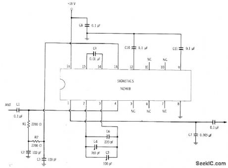
Single phase-locked loop IC provides audio output signal when connected to suitable antenna for broadcast band. Demodulation is achieved without use of input tuned circuits because control oscillator of PLL is locked to frequency of incoming carrier. IC is tuned over broadcast band by changing frequency of internal VCO with external variable capacitor 04. By changing capacitor limits, circuit can be used to cover long-wave and shortwave bands.-E. M. Noll, Linear IC Principles, Experiments, and Projects, Howard W. Sams, Indianapolis, IN, 1974, p 303-305. (View)
View full Circuit Diagram | Comments | Reading(1713)
LOGIC_CONTROLLED_RAMP_RATE
Published:2009/7/13 6:10:00 Author:May

Bidirectional linear ramp generator uses FET switch to slow ramp. With FET off, fast ramp has duration of 100 ms. With FET on, slow ramp is 1 s.-R.W. Currell, Linear Bidirectional Ramp Generator, EDN|EEE Magazine, Nov. 1, 1971, p 50-51. (View)
View full Circuit Diagram | Comments | Reading(1267)
200_MC_GAIN_CONTROLLED_STAGE
Published:2009/7/16 2:51:00 Author:Jessie

Has gain of 17 db With typical noise figure of 3 db,24 db of forward gain control,and 33 db of reverse gain contral.-Texas Instruments Inc., solid-State Communications, McGraw-Hill, N,Y., 1966,p 218. (View)
View full Circuit Diagram | Comments | Reading(582)
LOGIC_LEVEL_CONVERTER
Published:2009/7/13 6:10:00 Author:May

Converts from +18/-8V logic levels of some frequency converters and other digital test equipment to commonly used 0/-6V logic levels of datalogging system.-C. M. Jackson, Logic-Level Converter, EEE, 12:9, p61. (View)
View full Circuit Diagram | Comments | Reading(1473)
2_m_LOW_NOISE_PREAMP
Published:2009/7/16 2:51:00 Author:Jessie

Combination of grounded-gate and grounded-source connections uses bridge arrangement for neutralizing feedback capacitance between gate and drain.Input impedance is transformed in parallel between gate and ground to provide necessary wideband characteristic. Noise figure is between 1 and 2 dB, with gain of about 15 dB. Circuit is unconditionally stable, and combines optimum matching for best noise, lowest input SWR, and high power gain.-U. Rohde, High Dynamic Range Two-Meter Converter, Ham Radio, July 1977, p 55-57. (View)
View full Circuit Diagram | Comments | Reading(709)
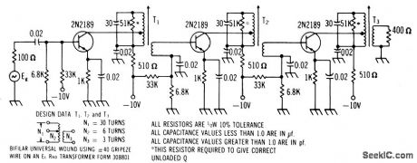
105_MC_I_F_WITH_2N2966
Published:2009/7/16 2:51:00 Author:Jessie
Proper loading gives good stability while providing 38 db power gain in two stages, with bandwidth of 8 Mc and noise figure of 2.5 db.-Texas Instruments Inc., Solid-Slate Communications, McGraw-Hill, N.Y., 1966, p 314. (View)
View full Circuit Diagram | Comments | Reading(593)
SIMPLEST_SWEEP_GENERATOR
Published:2009/7/13 6:09:00 Author:May

Requires only constant-current generator CR1, Schottky diode CR2, and capacitor. Provides excellent linearity (0.07%) and stability over wide range of supply voltages and temperatures. Sweep rates as high as 100 kHz can be obtained by changing value of C. Article gives design equations.-DR Morgan, Sweep Generator Boasts Only Three Parts, EDN Magazine, Sept. 15, 1970, p 57. (View)
View full Circuit Diagram | Comments | Reading(749)
REFERENCE_VOLTAGE_FOR_DIGITAL_CONVERTER
Published:2009/7/13 6:08:00 Author:May

Rectifies speech signals over 30.db range, and allows charge of memory capacitor to rise in millisec when speech input is applied, to form reference input voltage to digital converter for ratio quantizing unit.-J. D. Howells, Better Speech Quantizing for Pulse-Code Modulation, Electronics, 35:48, p 84-88. (View)
View full Circuit Diagram | Comments | Reading(1228)
RESONANT_FLUXGATE_MAGNETOMETER
Published:2009/7/13 6:06:00 Author:May

The core will get switched in the out of saturation. The output duty cycle varies in proportion to single-axis field strength and direction. The high-level output square wave is easy to interface to a PIC or other microcontroller. (View)
View full Circuit Diagram | Comments | Reading(1700)
MAGNETIC_FIELD_METER_
Published:2009/7/13 6:05:00 Author:May
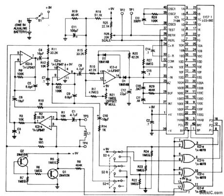
The meter's 12-turn field pickup is integrated into the unit's circuit board. For remote sensing, an external field coil probe can be used. The magnetic field picked up by the coil appears as a voltage, which is proportional to field strength and frequency at the input of a cascaded amplifier IC3-a, IC3-b, and IC3-c. With a first-stage amplifier gain of 3.3 set by R12 to R10, the overall sensitivity is 100 μV/μT, or 100 mV/mT. The meter sensitivity is nominally 2 V full scale, leading to the lowestlevel sensitivity of 20 mT full scale. Op amp IC3-a amplifies the signal to a normalized level of 100 μV/μT. The voltage is further amplified by 1, 100, or 10,000 by IC3-b and IC3-c. The three amplifier stages provide the ranges of 2 mT,200 μT, and 2 μT (full scale). Components R3 and C3 and R12 and C7 establish a frequency rolloff characteristic that compensates for the frequency-proportional sensitivity of the pickup coil, and set the 20-kHz cutoff point. IC3-d is a precision rectifier and peak detector. Its output drives IC1, a combination analog-to-digital (A/D) converter and LCD driver. Components R25 to R29 and C13 to C17 are used by IC1 to set display-update times, clock generation, and reference voltages. The decimal points are driven by IC2, as determined by range-select switch S2. Transistors Q1 and Q2 serve as a low-batterydetector, and turn on the battery annunciator in the LCD when the battery voltage drops below 7 V. (View)
View full Circuit Diagram | Comments | Reading(2412)
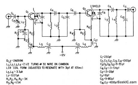
450_MC_TO_30_MC
Published:2009/7/13 6:05:00 Author:May

With local oscillator feeding 1 mw,conversion gain is 15 db and noise figure 10 db.With 2N2415 r-f stage ahead of mixer.combined power gain is 25db and noise figure 6 db.-Texas instruments Inc, Solid-State communications. McGawHill,N,Y.1966,p302. (View)
View full Circuit Diagram | Comments | Reading(509)
LINEAR_RAMP
Published:2009/7/13 6:04:00 Author:May

Free-running ramp generator has excellent linearity and repetition rate independent of supply voltage. C2 is charged at constant current through a, and is discharged by Q2. R2 provides sync pulse during retrace. Repetition rate of ramp is controlled by R3, from about 100 to 4000 Hz. Output voltage is 10 V P-P, and sync pulse amplitude is 5 V P-P.-J. J. Nagle, Voltage Independent Ramp Generator, CQ, Sept. 1972, p 61 and 98. (View)
View full Circuit Diagram | Comments | Reading(0)
BIDIRECTIONAL_RAMP
Published:2009/7/13 6:04:00 Author:May

Originally used to vary reference voltage for DC servomotor to control acceleration and deceleration. R2 and C1 determine ramp rate, while R1 controls ramp amplitude. With values shown, output takes n s to ramp from 0 to 10 V.-R. W. Currell, Linear Bidirectional Ramp Generator, EDN|EEE Magazine, Nov. 1, 1971, p 50-51. (View)
View full Circuit Diagram | Comments | Reading(734)
15_RANGE_SWEEP
Published:2009/7/13 6:03:00 Author:May

Serves for adjusting tuned circuits, aligning IF strips, and checking filter characteristics. Uses Motorola MC4024 IC containing two separate voltage-controlled MVBRs with output buffer for each. Frequency of oscillation is determined primarily by single switch-selected external capacitor that gives choice of 15 frequency ranges, with frequency within each range varied by applying DC control voltage to one pin of IC. For 3.5-5 V of control voltage, linearity is good. Output waveform is 4 V P-P at lower frequencies, becoming triangular at higher frequency ranges. HEP S9001 programmable UJT generates sweep signal. Switch gives choice of 100 Hz or 1 kHz sweep. Buffer and 741 opamp then give exponential sweep from about -1 to +1 V after DC level is set to 0 by 25K pot, for horizontal input of CRO. Sweep signal is also fed to MVBRs through controls giving independent width and center frequency adjustments. Diodes are 1-A 50-PIY silicon, T1 is 6.3 V at 1 A.-W. C. Smith, An Inexpensive Sweep-Frequency Generator, QST, Oct. 1976, p 17-19. (View)
View full Circuit Diagram | Comments | Reading(1233)
INVERTING_POWER_AMPLIFIER
Published:2009/7/13 6:02:00 Author:May
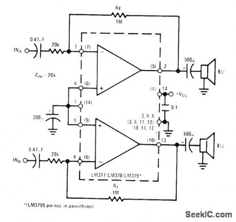
Single National LM377 IC provides 2 W per channel with 18-V supply for driving loudspeakers when fed by stereo demodulator of FM receiver. Similar LM378 chip gives 3 W per channel with 24-V supply, and LM379 gives 4 W per channel with 28-V supply. Gain is 50 for all. Heatsink is required.- Audio Handbook, National Semi-conductor, Santa Clara, CA, 1977, p 4-8-4-20. (View)
View full Circuit Diagram | Comments | Reading(0)
NONINVERTING_POWER_AMPLIFIER
Published:2009/7/13 6:01:00 Author:May


Single National LM377/LM378 provides gain of 50 and 3 W per channel for driving loudspeakers. Supply is 24 V. High input impedance permits use of high-impedance tone and volume controls. Heatsink is required,- Audio Handbook, National Semiconductor, Santa Clara, CA, 1977, p 4-8-4-20. (View)
View full Circuit Diagram | Comments | Reading(0)
PREAMP_WITH_TONE_CONTROLS_1
Published:2009/7/13 6:00:00 Author:May
Input stage is JFET having high input impedance and low noise. Circuit parameters are not critical, yet harmonic distortion level is less than 0.05% and S/N ratio is over 85 dB. Tone controls allow 18 dB of cut and boost. Input of 100 mV gives 1-V output at maximum level. Identical preamp is used for other stereo channel.- FET Data-book, National Semiconductor, Santa Clara, CA, 1977, p 6-26-6-36. (View)
View full Circuit Diagram | Comments | Reading(803)
D_C_TO_D_C
Published:2009/7/13 6:00:00 Author:May

Free-running multivibrator (250 kc) generates unidirectional square waves having amplitude of d-c input voltage. R-C circuit at output blocks average value of unidirectional pulse,and standard diode-capacitor voltage multiplier boosts output voltage to desired new value.-A. J. Durocher, D.c Voltage Converter Needs No Transforme, Electronics, 37:28, p 64-65. (View)
View full Circuit Diagram | Comments | Reading(712)
| Pages:691/2234 At 20681682683684685686687688689690691692693694695696697698699700Under 20 |
Circuit Categories
power supply circuit
Amplifier Circuit
Basic Circuit
LED and Light Circuit
Sensor Circuit
Signal Processing
Electrical Equipment Circuit
Control Circuit
Remote Control Circuit
A/D-D/A Converter Circuit
Audio Circuit
Measuring and Test Circuit
Communication Circuit
Computer-Related Circuit
555 Circuit
Automotive Circuit
Repairing Circuit