
Circuit Diagram
Index 681
SINGLE_POSITIVE_PULSE_GATES_SINE_WAVE_SIGNAL
Published:2009/7/16 2:19:00 Author:Jessie

Two transistors act as balanced shorting switch, eliminating pedestal effects that normally necessitate dual-polarity gate pulses for analog signal. Positive 10-V pulse saturates both transistors, thereby grounding both output terminals to give isolation from input signal. Analog signal being gated can be as low as 5-mv rms.-L. E. Frenzel, Jr., Gate Circuit Eliminates Pedestal Effects, Electronics, 37:15, p 77. (View)
View full Circuit Diagram | Comments | Reading(661)
_STARTER_CUTOFF
Published:2009/7/13 21:26:00 Author:May
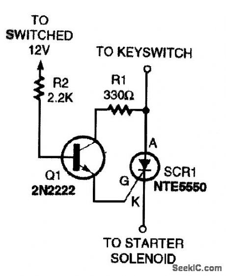
In this auto-starter cutoff circuit,two conditions are required to start the car∶The keys switcht must be turned to the starting position, and Q1 must be turned on When Q1 is switched to the ON state,current flOWS through the gate,allowing current to pass through the SCR,provided that the key switchis also turned to the starting position Transistor Q1 can be turned on by connecting R2 through a separate switch to a 12-V power Source or by usmg an existing switched Source Examples of existing Sources might be a brake light,turn signal, parking light,or anything that most people would not normally activate while starting a vehicle With regard to usmg a turn-signal indicator,it doesn’t matter that the power applied to Q1 is not constant Only a pulse IS required to latch the SCR on,provided that the key switch is in the starting position The SCR is a 25-A,50-V unit. (View)
View full Circuit Diagram | Comments | Reading(774)
70_MC_NEUTRALIZED_GAIN_CONTROLLED_AMPLIFIER
Published:2009/7/16 2:18:00 Author:Jessie

Gain is 27 db, with typical noise figure below 3 db. RC for reverse gain control is 0 ohms, and for forward gain control is 1,000 ohms. Reverse control range is 35 db, and forward gain control is 47 db.-Texas Instruments Inc., Solid-State Communications, McGraw-Hill, N.Y., 1966, p 215. (View)
View full Circuit Diagram | Comments | Reading(739)
PUMPED_TUNNEL_DIODE_LOGIC_GATES
Published:2009/7/16 2:18:00 Author:Jessie

Shows method of interconnecting negative-input positive-output gate with positive-input negative-output gate for high-speed computer logic.- Transistor Manual, Seventh Edition, General Electric Co., 1964, p 370. (View)
View full Circuit Diagram | Comments | Reading(791)
AND_GATE
Published:2009/7/16 2:17:00 Author:Jessie

Uses nor logic with inversion.- Transistor Manual, Seventh Edition, General Electric Co., 1964, p 179. (View)
View full Circuit Diagram | Comments | Reading(1730)
MOS_DRIVE_FOR_TRIAC
Published:2009/7/13 21:26:00 Author:May

Circuit uses one section of MC75492 hex buffer to boost 0.5-mA output of CMOS logic gate to 10 mA required for LED at input of Motorola MOC3011 optically coupled triac driver. When MOS input goes high, optoisolator provides output voltage for triggering triac that controls AC load. R is 220 ohms for 5-V supply and 600 ohms for 10-V supply. For 15 V, use MC14049B buffer and 910 ohms for R.-P. O'Neil, Applications of the MOC3011 Triac Driver, Motorola, Phoenix, AZ, 1978, AN-780, p 4. (View)
View full Circuit Diagram | Comments | Reading(1846)
VOLTAGE_CONTROLLED_GAIN
Published:2009/7/16 2:17:00 Author:Jessie

Response of two-transistor a-c amplifier, controlled by d-c voltage, can be mode linear by adding suitable feedback. With no d-c control voltage on base of Q1, both transistors are saturated, and effective shunt resistance of circuit is about 500,000 ohms, When d-c control voltage is increased positively until Q1 is cut off, effective shunt resistance drops to 200,000 ohms.-L. C. Bowers, Attenuator Controls Amplifier Gain, Electronics, 34:39, p 150-153. (View)
View full Circuit Diagram | Comments | Reading(0)
15_W_ADD_ON
Published:2009/7/13 21:26:00 Author:May

Increases usual 1-W audio output of transceiver to up to 15 W. Loudspeaker can be 8-ohm unit, but output will be somewhat reduced. -P. Bunnell, More Fun with the IC-230, 73 Magazine, May 1975, p 45-46 and 48. (View)
View full Circuit Diagram | Comments | Reading(680)
ONE_SHOT_LOGIC_CONTROLS_TRANSMISSION_GATE
Published:2009/7/16 2:17:00 Author:Jessie

Frequency generator, activated by negative pulse at A, generates 32-Mc burst in which number of cycles depends on input pulse width. Pushbutton-controlled one-shot logic allows diode transmission gate lo pass first complete 32-Mc burst occurring after pushbutton is actuated, after which gate is closed. One-shot has sync connection to pulse generator.-V. Kenn, One-Shot Gating Circuit Generates Sinewaves lot Testing Counters, Electronics, 34:23, p 114-116. (View)
View full Circuit Diagram | Comments | Reading(845)
HARD_LIMITING_OPAMP
Published:2009/7/13 21:25:00 Author:May

Based on limited output swing of opamp. Single pot adjusts both positive and negative limit points. First opamp produces limiting. Second opamp serves as voltage follower for isolating attenuator and redueing output impedance. Matching of output between limit points is within about 100 mV at output level of 2 V P-P. Opamps specified are adequate for 3-kHz bandwidth.-E. E. Bames, Ease Hard-Limiter Design with Op Amps, EDN Magazine, Aug. 5, 1975, p 76. (View)
View full Circuit Diagram | Comments | Reading(1690)
CASCADED_AGC
Published:2009/7/16 2:15:00 Author:Jessie

Double-conversion i-f uses two separate agc amplifiers to get good temperature stability and low noise figure with transistor amplifiers.-J. S. Brown, Improving Gain Control of Transistor Amplifiers, Electronics, 34:17, p 108-110. (View)
View full Circuit Diagram | Comments | Reading(841)
ANTIDUPLICATION_CIPCUIT
Published:2009/7/13 21:25:00 Author:May
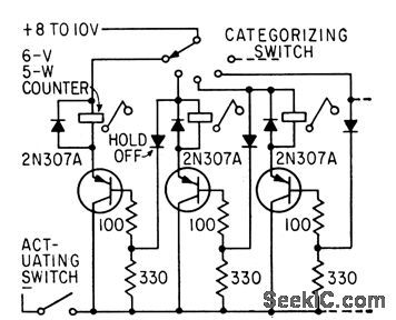
Diodes absorb flyback and prevent duplicate counts when categorized information ;is fed to banks of electromechanical counters.-R. L. lves , Reducing Errors in Category Counters, Electronics, 35:23, p 54-57. (View)
View full Circuit Diagram | Comments | Reading(964)
55_MC_CRYSTAL_OSCILLATOR_GATE
Published:2009/7/16 2:13:00 Author:Jessie

Provides train of pulses to be recd by 7-digit binary counter. Number of pulses in train depends on width of gate pulse received from gate amplifier, and is proportional to amplitude of data input pulse.-W. W. Grannemann et al, Pulse-Height-to-Digital Signal Converter, Electronics, 33:2, p 58-60. (View)
View full Circuit Diagram | Comments | Reading(477)
AM_SUBSYSTEM
Published:2009/7/16 2:13:00 Author:Jessie

Single RCA CA3088E IC serves as AM converter, IF amplifier, detector, and preamp for AM broadcast or communication receiver. RF amplifier stage using RCA 40841 dual gate-protected MOSFET is optional. IC also provides internal AGC for first IF stage and delayed AGC for optional RF stage. Internal buffer stage can be used to drive tuning meter.- Linear Integrated Circuits and MOS/ FET's , RCA Solid State Division, Somerville, NJ, 1977, p 348-349. (View)
View full Circuit Diagram | Comments | Reading(1228)
COMBINATION_GATE_AND_ONE_SHOT
Published:2009/7/16 2:12:00 Author:Jessie

Uses two four-layer switching diodes, and draws no current from source except during gate pulse. Can also be used as one-shot. Width of pulse depends on supply voltage and R5-C2.-R. E. Amsterdam, Gate/One. Shot Uses Four-Layer Diodes, EEE, 12:12, p 58-60. (View)
View full Circuit Diagram | Comments | Reading(515)
NPN_SERIES_TRANSISTOR_GATE_1
Published:2009/7/16 2:12:00 Author:Jessie

Circuit is and gate if closing of switch is an input. Circuit is or gate if opening of switch is an input. Provides phase inversion of input.- Transistor Manual, Seventh Edition, General Electric Co., 1964, p 176. (View)
View full Circuit Diagram | Comments | Reading(652)
SIMPLE_PLL_DEMODULATOR
Published:2009/7/16 2:11:00 Author:Jessie
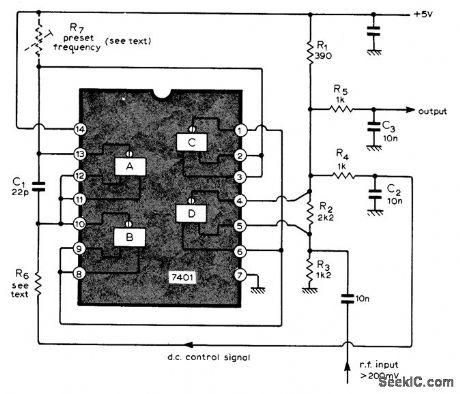
Requires only single IC to provide synchronous detection. Performance is satisfactory for most requirements of most amateur radio experimenters. Gates A, B, and C in IC form relaxation-type VCO whose output frequency is determined by C1 and positive current sources supplying pins 10 and 13 of IC. When pin 6 is high, gate D is biased by R2 and R3 to operate as linear amplifier for input signal. In operation, pin 6 is made alternately high and low by oscillator output, so D acts as amplifying phase detector. Output goes through low-pass filter R4-C2 to VCO, completing phase-locked loop. Separate filter R5-C3 provides AF output. When C1 is 22 pF, circuit operates at about 10 MHz. With 270 ohms for R6, lock is maintained over range of 2 MHz; with 10 kilohms, locking range is 300 kHz. R7 is optional, for fine adjustment of frequency.-R. King, Phase-Locked Loop Demodulator, Wireless World, July 1973, p 337. (View)
View full Circuit Diagram | Comments | Reading(839)
PNP_SERIES_TRANSISTOR_GATE
Published:2009/7/16 2:11:00 Author:Jessie

Circuit is or gate if closing of switch is an input. Circuit is and gate if opening of switch is an input. Provides phase inversion of input.- Transistor Manual, Seventh Edition, General Electric Co., 1964, p 176. (View)
View full Circuit Diagram | Comments | Reading(1202)
SYNCHRONIZED_GATE
Published:2009/7/16 2:10:00 Author:Jessie

Continuous train of pulses is applied to control grid of gating tube. When S1 is closed, next pulse in train opens gate, then shuts gate after itself.-J. K. Goodwin, Time and Pulses Control Gates, Electronics, 32:3, p 72-73. (View)
View full Circuit Diagram | Comments | Reading(662)
TWIN_PHANTASTRON
Published:2009/7/16 2:10:00 Author:Jessie

Frequency of free.-running twin-phantastron oscillator V3-V4 varies with controlled voltage ES (upper right). V5 gates starting pulses to phantastron when-ever it fails to oscillate. Used to generate train of pulses that continues in synchronism with incoming video data even when sync pulse is missing or below noise level-W. C. Whitworth, Plate Voltage Control of Phantrastron Frequency, Electronics, 34:6, p 73-74. (View)
View full Circuit Diagram | Comments | Reading(1434)
| Pages:681/2234 At 20681682683684685686687688689690691692693694695696697698699700Under 20 |
Circuit Categories
power supply circuit
Amplifier Circuit
Basic Circuit
LED and Light Circuit
Sensor Circuit
Signal Processing
Electrical Equipment Circuit
Control Circuit
Remote Control Circuit
A/D-D/A Converter Circuit
Audio Circuit
Measuring and Test Circuit
Communication Circuit
Computer-Related Circuit
555 Circuit
Automotive Circuit
Repairing Circuit