
Circuit Diagram
Index 700
TWO_INPUT_PINO_NOR_GATE
Published:2009/7/16 3:40:00 Author:Jessie

Pumped solid-state logic for uhf shift register using positive input-negative output gate gives 2-gc rate.-Tunnel Diode-Transistor Provides Fast Logic, Electronics, 35:11, p 72. (View)
View full Circuit Diagram | Comments | Reading(512)
432_MHz_TO_28_MHz
Published:2009/7/16 3:39:00 Author:Jessie

Contains bandpass filter, grounded-grid RF amplifier stages Q15-Q16,mixer Q17、and crystal oscillator Q18-Q19,Developed for use in all-band double-conversion superheterodyne receiver for AM narrow-band FM, CW, and SSB operation. Supply is 13.6 V regulated Article gives all circuits of receiver,-D. M. Eisenberg, Build This All-Band VHF Receiver 73Magazine, Jan 1975、p 105-112 (View)
View full Circuit Diagram | Comments | Reading(4104)
TRIGGERED_SQUARE_WAVE_GENERATOR
Published:2009/7/16 3:39:00 Author:Jessie

Synchronizing trigger signal drives phase splitter Q1, which in turn feeds blocking oscillator Q2. Output from emitter-follower Q3 is 1-microsec-wide pulse into 90-ohm load. Depending on connections for Q1, either positive or negative input pulse greater than 5 v will trigger generator. Maximum prr is 40 kc.-R. E. Daniels and C. Swoboda, Pulse Generator for Synchronizing Events, Electronics, 33:24, p 63. (View)
View full Circuit Diagram | Comments | Reading(1119)
2_SEC_TO_10_MIN_TIMER
Published:2009/7/16 3:39:00 Author:Jessie


Number of monolithic diode-transistor logic circuits determines range of time delay provided by potentiometer R7. For shorter delays, one or both of integrated circuits connected with broken lines may be eliminated.-A. A. Lampell, Off-the-Shelf Integrated Circuits for Versatile and Accurate Timer, Electronics, 38:25, p 70-73. (View)
View full Circuit Diagram | Comments | Reading(696)
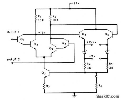
2_AND_4_INPUT_PULSE_NOR_GATE
Published:2009/7/16 3:39:00 Author:Jessie

Circuit is special-purpose nor gate for computer, control, and communication equipment. Used for the and operation when a general-purpose nor gate would be unsatisfactory because of possible spurious pulses in output.-NBS, Handbook Preferred Circuits Navy Aeronautical Electronic Equipment, Vol. II, Semiconductor Device Circuits, PSC 8 (originally PC 211), p 8-2. (View)
View full Circuit Diagram | Comments | Reading(670)
SIMPLE_INDUCTANCE_METER
Published:2009/7/16 3:38:00 Author:Jessie

This figure shows the schematic diagram of the simple inductance meter. U1, a 74LS00 two-input quad NAND gate logic integrated circuit, two resistors, a capacitor, and a surplus microprocessor crystal form a stable crystal oscillator near the marked frequency of the crystal. The RF voltage is taken from pin 8 through isolation capacitor C3 to the measuring circuit. RF voltage is applied through capacitor C7 to J1, a bindiftg post. This same RF voltage is applied to a resistive voltage divider consisting of R3 and R4. Germanium diode D1 has its anode connected to the junction between R3 and R4. RF across the variable tuning capacitor C6 is applied back through C5 to the cathode of D1 and load resistor R5, the lower end of which is bypassed to ground through C4 and applied to the positive terminal of meter M1. R6 is a sensitivity control connected between the negative terminal of meter M1 and ground. This instrument operates by measuring the RF voltage developed across C6, which will be the highest when the series circuit made up of C6 and the unknown inductance is at resonance at the crystal frequency. In other words, the value of the unknown is indicated on the dial attached to C6 when the voltage indicated by M1 peaks, just the opposite of bridge operation. (View)
View full Circuit Diagram | Comments | Reading(5995)
DARLINGTON_INPUT_OPERAIIONAL_AMPLIFIER
Published:2009/7/16 3:38:00 Author:Jessie
Single-stage version uses emitter-follower output to lower impedance and shift d-c level of output. Q7 and R3 form constant-current source. Zeners, formed as base-emitter junctions of transistors, shift d-c level of outputs negative by 6 V to make them compatible with input voltages and permit cascading of monolithic integrated circuits directly.-C. L. Heizman and D. G. Paterson, Circuit Analysis: A Monolithic Integrated Operational Amplifier, EEE, 13:5, p 80-84. (View)
View full Circuit Diagram | Comments | Reading(827)
DRIVERS_FOR_SHIFT_REGISTER
Published:2009/7/16 3:37:00 Author:Jessie

Inverter Q3 pulses 300-ma drivers Q1 and Q2 and feeds 100-nsec delay line that provides time for shift register stages to reach final values in new stale.-B. K. Ericksen and J. D. Schmidt, Random Pulse Generator Tests Circuits, Encodes Messages, Electronics, 34:25, p 56-59. (View)
View full Circuit Diagram | Comments | Reading(551)
IMPROVED_DARLINGTON
Published:2009/7/16 3:37:00 Author:Jessie

Separate collector circuit for, third Transistor of Darlington configuration prevents refection of high capacitance back to input, thereby dissipating Miller effect.-Y. Tarui, Japan Seeks Its Own Route to Improved IC Techniques, Electronics, 38:25, p 90-98. (View)
View full Circuit Diagram | Comments | Reading(611)
QUICK_DISCONNECT_TACHOMETER
Published:2009/7/16 3:37:00 Author:Jessie
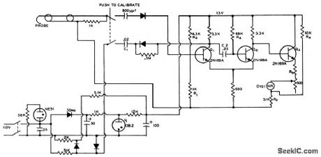
Can be connected and disconnected from engine fast enough for production-line speed adjustments. Pulse is picked up by curved probe that is hooked over ignition cable in use. Probe is made from RG58A/U coax with 1 inch of shield removed to provide coupling. Resulting pulse picked up is about 1 v, with width of about 20 microsec. Pulse is fed lo first stage Q1 of monostable mvbr, which acts on Q2 to give pulse with constant height and width, having engine spark frequency. Meter gets current pulse through emitter-follower for each spark, so average meter current is proportional to rpm.-Transistorized Tachometer, Electronic Circuit Design Handbook, Mactier Pub. Corp., N.Y., p 154. (View)
View full Circuit Diagram | Comments | Reading(751)
28_30_MHz_TO_165_MHz
Published:2009/7/16 3:37:00 Author:Jessie

10-meter tuner gives excellent image suppression with 1.65-MHz output, for feeding into inexpensive receiver having 1.65.MHz IF. Tuning capacitors are three-gang Miller 1460-1. Article gives all coil data along with construction details.-B. Hoisington, Tuneable 10 Meter Converter, 73 Magazine, Jan, 1974, p 57-62. (View)
View full Circuit Diagram | Comments | Reading(1289)
DUAL_4_INPUT_GATE
Published:2009/7/16 3:37:00 Author:Jessie

Each 4-input section uses 4-transistor chip for hybrid microelectronic construction.-J. G. Curtis, Crossbred Technology Automates Production of Hybrid Microcircuits, Electronics, 38:13, p 66-73. (View)
View full Circuit Diagram | Comments | Reading(633)
THREE_OUTPUT_PRF_GENERATOR
Published:2009/7/16 3:36:00 Author:Jessie
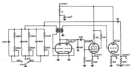
Switch gives choice of 200, 300, and 800 pps. Output C is negative, and other outputs are positive. Output B has positive overshoot to provide trigger that is delayed with respect to out-puts A and C by width of pulse.-NBS, Handbook Preferred Circuits Navy Aeronautical Electronic Equipment, Vol. l, Electron Tube Circuits, 1963, p N5-2. (View)
View full Circuit Diagram | Comments | Reading(773)
ASTABLE_MVBR
Published:2009/7/16 3:36:00 Author:Jessie

Stress-sensitive RC103 integrated circuit shifts free-running frequency from 500 kc to 1 Mc when 7 grams of force is applied to one transistor.-R. C. Wonson, Stress- Sensitive Integrated Circuits, Electronics, 38:14, p 81-84. (View)
View full Circuit Diagram | Comments | Reading(599)
DIODE_COUPLED_NAND_NOR_GATE
Published:2009/7/16 3:36:00 Author:Jessie

Designed for integrated circuits, arrangement gives unlimited fan-in and high immunity to noise, with 1.7 v logic swing.-A. E. Skoures, Choosing Logic for Microelectronics, Electronics, 36:40, p 23-26. (View)
View full Circuit Diagram | Comments | Reading(595)
MONOSTABLE_MVBR
Published:2009/7/16 3:36:00 Author:Jessie

Pulse width of stress-sensitive RC103 integrated circuit is reduced from 1.5 to 1.0 microsec when 7 grams of force is applied to one transistor-R. C. Wonson, Stress-Sensitive Integrated Circuits, Electronics, 38:14, p 81-84. (View)
View full Circuit Diagram | Comments | Reading(645)
MAGNET_ACTUATED_IGNITION
Published:2009/7/16 3:35:00 Author:Jessie
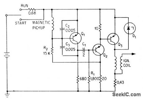
Distributor contact points are replaced by magnetic pickup that delivers timed pulses to trigger transistor Q1, driver Q2 and output transistor Q3, with latter controlling primary current through ignition coil. Zenet diode D1 clips voltages exceeding voltage rating of Q3.-S.B. Gray, Home and Auto Controls, Electronics, 36:19, p 52-56. (View)
View full Circuit Diagram | Comments | Reading(2867)
BELOW_BROADCAST_BAND
Published:2009/7/16 3:35:00 Author:Jessie

Simple solidstate converter can be used with any good communication receiver covering 3.5-4 MHz to bring in stations from 5-550 kHz (200 meters and up). Input coil L1 is changed from 0.28 H for 5-11 kHz to 120 μH for 250-550 kHz in eight steps, as given in article. C2 consists of two 3-gang variable capacitors with stators wired in parallel, gang-tuned with dial cords. Trimmer C7 is 1-12 pF, adjusted to give reliable starting of FT-2433500-kHz crystal. L2 is 80-90 μH for 80 meters, and loopstick is for broadcast band. -K. Cornell, 200 Meters and Up Receiving Converter for Low Frequencies, Ham Radio, Nov. 1976, p 24-26. (View)
View full Circuit Diagram | Comments | Reading(1286)
COMPLEMENTARY_RDTL_NOR
Published:2009/7/16 3:35:00 Author:Jessie

Alternately provides 500-na base current to pnp and npn transistors, thereby using transistor rise time at both edges of switching pulse to eliminate R-C time constant fall times of output wave form. Design reduces power drain and speeds up rise and fall times by factor of 15.-R. A. Tietsch, Complementary Microwatt Logic Circuits, EEE, 11:8, p 51-52. (View)
View full Circuit Diagram | Comments | Reading(612)
AVALANCHE_SWITCH
Published:2009/7/16 3:35:00 Author:Jessie

Low-cost germanium transistors used in avalanche mode provide narrow pulses with fast rise times. Width of input pulse determines number of output pulses. For testing counter, collector voltage of Q2 was adjusted for ten pulses per input pulse, at input repetition rate of up to 100,000 pps.-B. S. Ahn, Germanium Transislor As Avalanche Switch, Electronics, 37:30, p 44. (View)
View full Circuit Diagram | Comments | Reading(913)
| Pages:700/2234 At 20681682683684685686687688689690691692693694695696697698699700Under 20 |
Circuit Categories
power supply circuit
Amplifier Circuit
Basic Circuit
LED and Light Circuit
Sensor Circuit
Signal Processing
Electrical Equipment Circuit
Control Circuit
Remote Control Circuit
A/D-D/A Converter Circuit
Audio Circuit
Measuring and Test Circuit
Communication Circuit
Computer-Related Circuit
555 Circuit
Automotive Circuit
Repairing Circuit