
Circuit Diagram
Index 680
POSITIVE_TRANSMISSION_GATE
Published:2009/7/16 2:23:00 Author:Jessie
Is equivalent to digitally controlled analog switch, for frequency range of 8 to 650 kc. Output signal never passes through active device, hence is not attenuated, distorted, or delayed. Will pass a-c signal with zero aver age value. Ratio of on voltage to off voltage is 420:1 (4.2 V pp to 10 mV p-p), for isolation of 54.5 db.-V. A. Bloom, Positive Transmission Gate, EEE,10;9, p 26-27. (View)
View full Circuit Diagram | Comments | Reading(574)
FAST_READOUT_MEMORY
Published:2009/7/16 2:22:00 Author:Jessie
Voltage-divider version of tunnel-diode gate is used with toroid to give extremely fast readout, for use with computers having dock rates above 500 Mc. Tertiary winding cancels gating spike.-F. W. Kantor, Tunnel-Diode Gate has Subnanosecond Rise Time, Electronics, 35:15, p 62-64. (View)
View full Circuit Diagram | Comments | Reading(587)
450_MC_GAIN_CONTROLLED_STAGE
Published:2009/7/16 2:22:00 Author:Jessie

Has gain of 8 db with typical noise figure of 4 db. Reverse gain control is 21 db for collector current of 20 microamp, and forward gain control is 26 db at 7 ma collector current.-Texas Instruments Inc., Solid-State Communications, McGraw-Hill, N.Y., 1966, p 220. (View)
View full Circuit Diagram | Comments | Reading(581)
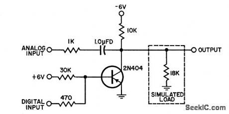
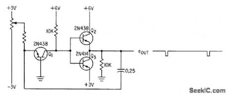
NPN_NOR_GATE
Published:2009/7/16 2:22:00 Author:Jessie
Circuit is or gate if dosing of switch is an input. Circuit is and gate if opening of switch is an input. Provides phase inversion of input. If both switches are open, both transistors are nonconducting. When either switch is dosed, output is negative, or not or, because of phase inversion, and circuit is therefore nor gate.- Transistor Manual, Seventh Edition, General Electric Co., 1964, p 176. (View)
View full Circuit Diagram | Comments | Reading(615)
SINGLE_SCS
Published:2009/7/16 2:22:00 Author:Jessie

R4 varies relaxation frequency of pnpn silicon controlled switch from 1 to 500 pps, independently of pulse duration and amplitude. For operation in gated mode, cathode gate pulse at input should be -1.5. v at 50 microamp.-H. H. Wieder, Silicon Controlled Switch Con Generate Pulses, Electronics, 38:2, p 79. (View)
View full Circuit Diagram | Comments | Reading(603)
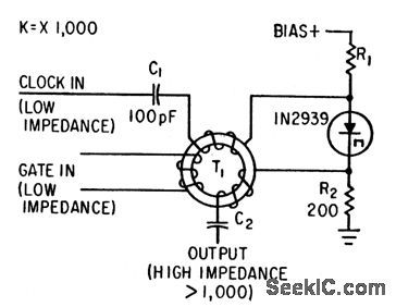
GATE_WITH_TAPPED_TOROID
Published:2009/7/16 2:21:00 Author:Jessie

Arrangement of toroid windings minimizes number of com ponents in ac bridge used as computer gate, while keeping gating pulse out of output.R3 adjusts balance. Bias is adjusted for stable switching.-F. W. Kantor, Tunnel-Diode Gate has Subnanosecond Rise Time, Electronics, 35:15, p 62-64. (View)
View full Circuit Diagram | Comments | Reading(616)
PHANTASTRON
Published:2009/7/16 2:21:00 Author:Jessie
Reversal of current and volt-age functions of basic three-transistor phantastron sweep generator results in pulse output that is derivative of sawtooth sweep.-N. C. Hekimian, Phantastron Circuits Using Transistors, Electronics, 34:8, p 46-47. (View)
View full Circuit Diagram | Comments | Reading(2161)
AUDIO_AGC_FOR_40_DB_RANGE
Published:2009/7/16 2:20:00 Author:Jessie

Automatic gain-adjusting amplifier produces constant output for speech level variations up to 40 db. Intelligibility of speech is ensured by allowing instantaneous peaks to remain.-L.E. Getgen, Amplifier Compensates for Speech-Level Variations, Electronics,33:31, p 103-106. (View)
View full Circuit Diagram | Comments | Reading(645)
TRIPLING_TO_12672_MHz
Published:2009/7/13 21:36:00 Author:May
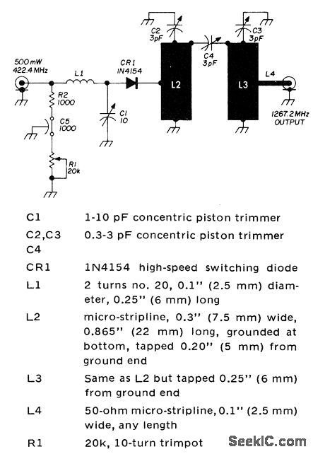
Diode tripler and filter combination is designed for double-clad glass epoxy printed-circuit board to simplify construction. Developed for use in 1296-MHz SSB transceiver for amateur 23-cm band. RF energy from 422.4-MHz power amplifier is applied to GE 1N4154 high-speed switching diode through L network .Harmonic comb at output of diode passes only desired frequency to output terminal going to mixer of transceiver. -H. P. Shuch, Easy-to-Build SSB Transceiver for 1296 HMz, Ham Radio, Sept. 1974, p 8-23. (View)
View full Circuit Diagram | Comments | Reading(637)
INFRARED_CURTAIN_BIRD_COUNTER
Published:2009/7/13 21:36:00 Author:May
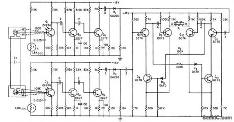
System registers appearance of bats and other moving objects moving through curtain of infrared light. Logic circuit determines direction of travel. Direction and pass time are automatically printed by mechanical register K1.-P. A. Tove and J. Czekajewski, infrared Curtain System Detects and Counts Moving Objects, Electronics, 34:31, p 40-43. (View)
View full Circuit Diagram | Comments | Reading(623)
BENCHTOP_FUNCTION_GENERATOR_WITH_BUILT_IN_COUNTER_
Published:2009/7/13 21:36:00 Author:May
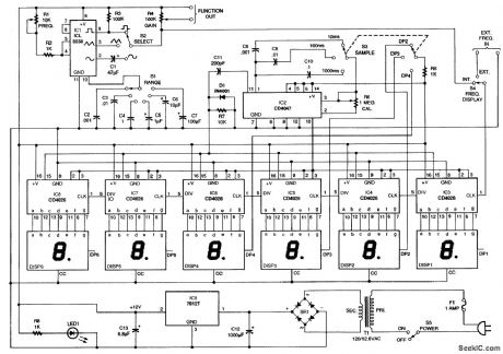
This circuit will produce sine, square, and triangle waves from 0.1 Hz to 1 MHz and has a counter which will read the frequency of the function generator or an external signal of a few volts peak-to-peak that will drive the CMOS counter. (View)
View full Circuit Diagram | Comments | Reading(3257)
ACTIVE_HIGH_TRIAC_INTERFACE
Published:2009/7/13 21:34:00 Author:May
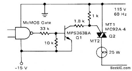
Typical CMOS logic gate operating from negative supply triggers triac on negative gate current of 8mA for control of 25-W AC load. High supply lines for both logic gate and interface transistor are grounded.-A.Pshaenich, Interface Techniques Between Industrial Logic and Power Devices, Motorola, Phoenix, AZ, 1975, AN-712A, p 12. (View)
View full Circuit Diagram | Comments | Reading(1091)
NE602_FREQUENCY_CONVERTER
Published:2009/7/13 21:32:00 Author:May
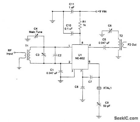


The NE602 can be used as a frequency converter with this circuit.
(View)
View full Circuit Diagram | Comments | Reading(2349)
NE602_DIRECT_CONVERSION_OUTPUT_CIRCUIT
Published:2009/7/13 21:30:00 Author:May
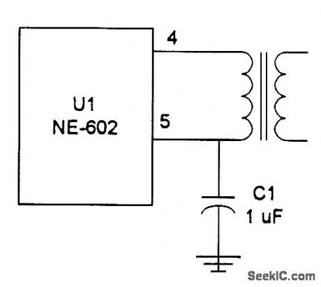
This figure shows a direct-conversion output circuit for an NE602. (View)
View full Circuit Diagram | Comments | Reading(527)
INVERTER_LIMITER
Published:2009/7/13 21:30:00 Author:May

Developed for direct-conversion receivers that lack AGC, to provide limiting for CW reception. Below adjustable limiting threshold, amplifier is linear with voltage gain of 10. When output is high enough for silicon diodes to conduct, gain drops below unity.Amplifier should be preceded by several sections of filtering and followed by single-section low-pass filter to eliminate harmonic distortions generated in limiting process.-W. Hayward, Simple Active Filters for Direct-Conversion Receivers, Ham Radio, April 1974, p 12-15. (View)
View full Circuit Diagram | Comments | Reading(539)
10_CHANNEL_SCANNER
Published:2009/7/13 21:29:00 Author:May

Designed for Regency HR-212 2-meter transceiver but can be adapted for other transceivers,Features include automatic stop, start, and large LED 7-segment readout. Diodes D1-D10 prevent transceiver voltages from reaching scanner circuit. Squelch voltage input of 2N3053 is taken from transceiver. S1-S10 are used to switch out channels not monitored. Wires going to chokes in HR-212 should be connected to choke leads going to channel switch.-A. Little, 10-Channel Scanner for the Regency HR-212, QST, Feb. 1978, p 37. (View)
View full Circuit Diagram | Comments | Reading(1351)
SIMPLE_SCANNER_CONVERTER
Published:2009/7/13 21:29:00 Author:May


This circuit can be powered from any 9- to 12-Vdc source, including a good alkaline 9-V battery.Switch S1 either puts the unit into its Bypass mode, where a scanner connected to J3 will receive its normal signals, or applies power to the circuit and down-converts all 800- to 950-MHz signals as follows: At the heart of the circuit is OSC1, a 40-MHz oscillator module. Transistor Q1 amplifies the oscillator's output, which is then bandpass filtered four times so that only the tenth harmonic at 400 MHz is presented to the input of U1, a Mini Circuits MAR1 wideband UHF/VHF amplifier. Signals from an antenna connected to J2 are high-pass filtered by capacitors C4 to C7 in conjunction with inductors L2 to L4. Those inductors are etched into the tracings on the PC board, making the exact PC board layout a necessity if the circuit is to function. Mixer U1 amplifies and mixes the two inputs-signals between800 and 950 MHz and the 400-MHz local oscillator-and passes the 400- to 550-MHz output to J3. This converter is not suitable for areas where signal strength is low or areas where a large number of strong signals are present, as no RE stage is used and little input filtering is used be-fore the mixer, making this circuit prone to spurious responses. (View)
View full Circuit Diagram | Comments | Reading(657)
“BAT_BAND”CONVERTER
Published:2009/7/13 21:27:00 Author:May

The full circuit diagram of the bat-band converter is shown. All components, with the exception of the transducer (X1), the ON/OFF switch, and the ferrite rod antenna, are surface-mount devices (SMDs). The signals from X1 are very small (microvolts, rather than millivolts). A low-noise FET input stage, TR1, has minimal loading effect on X1 and provides a low-impedance source for the passive high-pass filter. This simple filter consists of capacitors C1 and C2 and resistor R3. It attenuates signals below about 15 kHz, but the rolloff is very gradual. Mid-range and lower-frequency audio is strongly reduced. The falling sensitivity of transducer X1 further limits the audio frequencies reaching the mixer IC1. Despite this level of attenuation, a little audio still gets through the system, but it has no effect on the ultrasonic operation. When the receiver is tuned close to the 1-MHz local oscillator, a little audio feedback will be heard. This is a real help with tuning in because it readily identifies the low-frequency end of the bat band. The transistor TR2 is a low-noise amplifier, and the SMD-type BSX70H works well in this circuit. IC1 is a double-balanced mixer and Colpitts oscillator in one package. The signal inputs at pin 1 and pin 2 are used in unbalanced mode, with pin 2 decoupled by capacitor C4. (View)
View full Circuit Diagram | Comments | Reading(755)
ZERO_CROSSING_SWITCH_FOR_HEART_SOUNDS
Published:2009/7/16 2:20:00 Author:Jessie

Active filter with three amplifiers provides output pulse for opening sliding gate at instant when heart sound being monitored is zero. Filter has sharp cutoff above highest-frequency heart sound (600 cps.)-R. Weiss, Heart-Sound Discriminator Simplifies Medical Diagnosis, Electronics, 34:24, p 52-55. (View)
View full Circuit Diagram | Comments | Reading(597)
9_MHz_CRYSTAL
Published:2009/7/13 21:27:00 Author:May

Used in transmitter section of 80-meter 10-W SSB transceiver. Value of C1 is 50-330 pF, chosen for desired output range. Carrier level can be adjusted with slug-tuned coil or with 30K trimpot.-D. Hembling, Solid State 80-Meter SSB Transceiver, Ham Radio, March 1973, p 6-17. (View)
View full Circuit Diagram | Comments | Reading(1466)
| Pages:680/2234 At 20661662663664665666667668669670671672673674675676677678679680Under 20 |
Circuit Categories
power supply circuit
Amplifier Circuit
Basic Circuit
LED and Light Circuit
Sensor Circuit
Signal Processing
Electrical Equipment Circuit
Control Circuit
Remote Control Circuit
A/D-D/A Converter Circuit
Audio Circuit
Measuring and Test Circuit
Communication Circuit
Computer-Related Circuit
555 Circuit
Automotive Circuit
Repairing Circuit