
Circuit Diagram
Index 678
TR_CONTROL
Published:2009/7/13 21:43:00 Author:May

Used to control low-power transceiver for 20-meter amateur band. Sidetone is obtained from simple relaxation oscillator using GED-13-T programmable UJT. Sawtooth output is attenuated and applied to input of two-transistor audio amplifier. Transmitter keying is done with series switch using 2N4036 silicon transistor. Antenna relay applies +12 V appropriately to transceiver stages used during transmit (+12T) and receive (+12R), and provides switching of antenna between transmitter power chain and receiver RF amplifier. Use DPDT relay with 800-ohm 12-V coil. Transmit receive logic uses μA741C opamp as differential comparator. When key is closed, 2.2-μF capacitor is discharged, making opamp output switch to high state and saturate 2N3904 relay driver, pulling in relay for transmit operation. When key is released, capacitor begins to charge; at 6-V point (about 0.5 s with 220K timing resistor), opamp changes state again and relay opens for receiving.-W. Hayward, Low-Power Single Band CW Transceiver, Ham Radio, Nov. 1974, p 8-17. (View)
View full Circuit Diagram | Comments | Reading(735)
INFRARED_COMMUNICATIONS_TRANSCEIVER
Published:2009/7/16 3:12:00 Author:Jessie

When push-to talk Switch S6 is closed amplified microphone signal modulates Infrared output of tungsten lamp. Lens gives 1° beam. When switch is released, lead sulfide cell picks up radiation from another transceiver, for driving speaker or phones through audio preamp and audio amp.-P W. Kruse and L.D. McGlauchlin, Solid-State Modulators for Infrared Communications, Electronics, 34:10, p 177-181. (View)
View full Circuit Diagram | Comments | Reading(652)
45_MC_CASCODE_FET
Published:2009/7/16 2:38:00 Author:Jessie
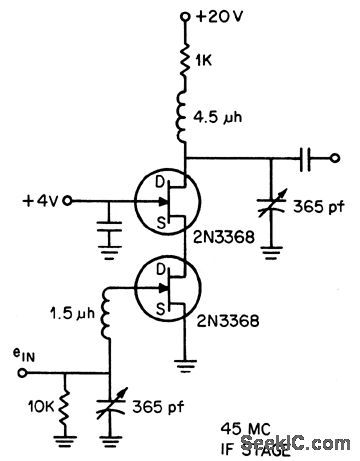
Operates without neutralization, giving 20 db power gain and 6-Mc bandwidth. -Cascode with FET's (Siliconix ad), Electronics, 39:2, p 109. (View)
View full Circuit Diagram | Comments | Reading(845)
ADF_DEGREE_INDICATING_COUNTER
Published:2009/7/13 21:42:00 Author:May

V1 is used in conventional pulse-forming circuit to drive counter V2.Each counter tube is connected to next by half of 12AT7. When first counter passes zero. Pulse at its output is fed to next conter. -J.F. Hatch and D.W.G. Byatt. Direction Finder with Automatic Readout. Electronics.32:16,p62-64 (View)
View full Circuit Diagram | Comments | Reading(499)
SLICER_AND_GATE_FOR_AGC
Published:2009/7/16 2:33:00 Author:Jessie

When peak-to-peak value of input signal exceeds preset reference voltage, slicer Q2 conducts, making Q4 apply amplified signal to Schmitt trigger for squaring. Q7 then delivers output ate that changes fixed-gain amplifier to unity gain to give effect of fast agc for monopulse radar amplifier.- W. W. Smith, Fast AGC Amplifier Locks Monopulse Radar on Target Electronics, 36:39, p 34-36. (View)
View full Circuit Diagram | Comments | Reading(601)
BIPOLAR_ZENER
Published:2009/7/13 21:42:00 Author:May
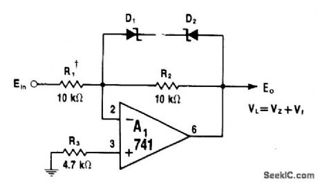
Circuit limits opamp output swing in either direction to sum of zener- and forward.breakdown voltages of D1 and D2. With matched zeners, positive and negative limiting levels are symmetrical. With 10-V zenets, limiting occurs at 10.6 V (10.0 + 0.6 V) to allow linear t 10 V swing without saturating A1. R2 is selected according to gain requirement. Diodes are matched pair chosen to provide desired limit voltage, such as 1N758 for ±10 V output swing.-W. G. Jung, IC 0p-Amp Cookbook, Howard W. Sams, Indianapolis, IN, 1974, p 201. (View)
View full Circuit Diagram | Comments | Reading(1214)
BRIDGE_TRIGGERED__TRIAC
Published:2009/7/13 21:41:00 Author:May

Developed for use with AC sensor in one leg of bridge. CA3094 is shut down on negative half-cycles of line. When bridge is unbalanced so as to make pin 2 more positive than pin 3, IC is off at instant that AC line swings positive; pin 8 then goes high and drives triac into conduction. Triac conduction is maintained on next negative half-cycle by energy stored in 100-μF capacitor. Bridge unbalance in opposite direction does not trigger triac.-E. M. Noll, Linear IC Principles, Experiments, and Projects, Howard W, Sams, Indianapolis, IN, 1974, p 313-314. (View)
View full Circuit Diagram | Comments | Reading(839)
SINGLE_TUNED_FINAL_I_F
Published:2009/7/16 2:33:00 Author:Jessie
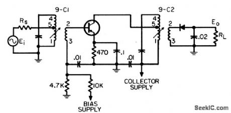
Circuit is example of optimum design based on use of transistor signal-handling curves. Transformers are single-tuned.-W. Rheinfelder, Using transistor Signal Handling Curves in Receiver Design, EEE, 14:6, p 62-66. (View)
View full Circuit Diagram | Comments | Reading(614)
4_CHANNELVHF_FM_SCANNER
Published:2009/7/13 21:40:00 Author:May
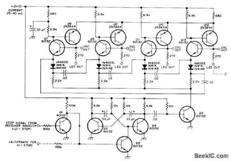
Discrete components permit simpler readout, with any number of channels and any desired scan rate. Operates directly from 10-15 V power supply without regulation, and has low current drain. Can be used with either positive or negative logic from squelch circuit, so scanning can be stopped with either positive or ground signal. Any voltage from a few volts up will stop scanning. Q3 and Q4 form astable MVBR operating at about 10 pulses per second. Q2 turns on to stop MVBR when base of Q2 is high. Inverter Q1 provides proper polarity of signal to operate Q2. Q6-Q13 form 4-stage ring counter. Pulsing by Q5 serves to pass high output from stage to stage in endless ring pattern. When squelch stops pulsing action, counter stops stepping and output of one counter stage stays high, providing 5-V output for enabling corresponding oscillator and driving LED for that channel, Article gives connections to oscillator for almost any FM transceiver or receiver, along with modifications for changing scan speed and number of channels.-J. Vogt, Improved Channel Scanner for VHF FMJ Ham Radio, Nov, 1974,p26-31. (View)
View full Circuit Diagram | Comments | Reading(1694)
OPTIMIZED_LOW_DISTORTION_I_F_AMPLIFIER
Published:2009/7/16 2:32:00 Author:Jessie

Provides 0.5 V audio from detector, with 3 db of control with agc. Volume control is diode detector load resistor. First i-f stage uses ceramic filters for sharper bandpass characteristic.-W. Rheinfelder, Using Transistor Signal Handling Curves in Receiver Design, EEE, 14:6, p 62.66. (View)
View full Circuit Diagram | Comments | Reading(634)
WHEATSTONE_RESISTANCE_BRIDGE
Published:2009/7/16 2:32:00 Author:Jessie
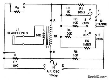
R7 is a calibrated potentiometer. At null, RX equal Rn(R7/R6),where Rn=R1,R2,R3,R4,or R5,as selected by switch S1. (View)
View full Circuit Diagram | Comments | Reading(814)
30_MC_GAIN_CONTROLLED_STAGE
Published:2009/7/16 2:31:00 Author:Jessie

Gain is 15db. Typical noise figure is 5db. Reverse gain control range is 25 db from collector current of 1.5 ma to 20 microamp. Provides 20 db of forward gain control.- Texas Instruments Inc., Solid-State Comunications, McGraw-Hill,N.Y.,1966, p 211. (View)
View full Circuit Diagram | Comments | Reading(607)
12_V_CROWBAR
Published:2009/7/13 21:39:00 Author:May
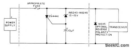
Uses overvoltage-sensing zener to trigger SCR and place it across power supply line, blowing fuse within microseconds to protect transceiver. Optional diode provides protection from accidental reversal of supply polarity.-Circuits, 73 Magazine, July 1977, p 35. (View)
View full Circuit Diagram | Comments | Reading(697)
GROUNDED_GRID_STRIP
Published:2009/7/16 2:31:00 Author:Jessie
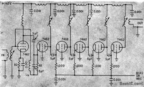
Six-stage low-noise 60-Mc i-f strip amplifier, using microminiature ceramic triodes, gives 75-db overall gain, 1.7-db noise figure, and 6.5.Mc bandwidth.First stage is cascode and other five are grounded-grid triodes.-J. W. Rush, Designing Grounded-Grid Amplifiers with Controlled Gain, Electronics, 33:52, p 50-53. (View)
View full Circuit Diagram | Comments | Reading(744)
AUTO_GUARDIAN_RECEIVER
Published:2009/7/13 21:38:00 Author:May
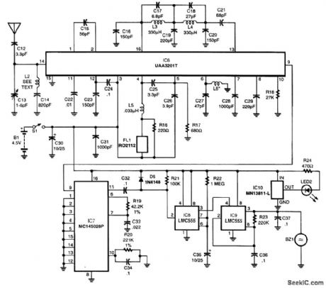
The decoder IC7 cheeks the incoming pulse train for the correct address. If that address is present, the valid output terminal, pin 11, goes high for the 2 1/2-s duration of the transmitted pulse trains. When the valid output signal returns to a low state, timer lC8 is triggered into operation. The output terminal of IC8, pin 3, goes high for a time period of about 11 s, as determined by R22 and C35. That output, in turn, enables IC9, a timer configured as a 50-percent duty-cycle oscillator with a period of about 1/4 s. The output of IC9 drives a piezo buzzer, which produces an attention-getting audio signal that alerts the user that a door of the vehicle has been opened. Power to operate the receiver is obtained from a set of three AAA alkaline cells connected in series to produce 4.5 V. Current draw is only 3 mA during standby, so battery life will be in the hundreds of hours. IC10 is a voltage-detector IC that allows current to flow through LED2 when the battery voltage falls below 3 V. That alerts the user that battery replacement is necessary. (View)
View full Circuit Diagram | Comments | Reading(626)
500_MC_STAGGER_TUNED_I_F
Published:2009/7/16 2:30:00 Author:Jessie
Slight staggering in two stages gives excellent stability, so circuit will not oscillate when either source or load is open. Bandwidth is 90 Mc for 1 db down and 110 Mc for 3 db down, with midband gain of 21 db. Draws only 7 mc at 15 V.-Texas Instruments Inc., Solid-State Communications, McGraw-Hill, N.Y., 1966, p 315. (View)
View full Circuit Diagram | Comments | Reading(640)
TWO_CHIP_LOW_COST_STRIP
Published:2009/7/16 2:30:00 Author:Jessie
Detector and 10.7-Mc i-f strip give 95 db gain. Differential amplifier in both RCA chips provides symmetrical limiting over wide input voltage range. Audio output is 220 my.-R. L. Sanquini, Integrated Circuits Make A Low-Cost F-M Receiver, Electronics, 39:16, p l33-138. (View)
View full Circuit Diagram | Comments | Reading(865)
30_MC_GAIN_CONTROLLED_TETRODE
Published:2009/7/16 2:29:00 Author:Jessie

Collector voltage and current are kept constant and gain is changed in accordance with base-2 current. Gain is 21 db and typical noise figure is 6O db,-Texas Instruments Inc., Solid-State Communications, McGraw-Hill, N.Y., 1966,p 213. (View)
View full Circuit Diagram | Comments | Reading(638)
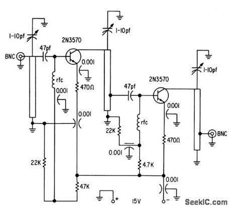
2_23_MHz_UNTUNED_OSCILLATOR
Published:2009/7/13 21:37:00 Author:May

Two dualgate MOSFETs operate in untuned Colpitts crystal oscillator Used in SSB transceiver made by Sideband Associates for radiomarine communication in 2-23 MHz range Oscillator feeds isolating amplifier,Small capacitor can be used for netting individual crystal to precise assigned frequency.-E Noll, MOSFET Circuits, Ham Radio Feb 1975,p50-57. (View)
View full Circuit Diagram | Comments | Reading(1323)
I_F_TUNING_WITH_DELAY_LINE
Published:2009/7/16 2:29:00 Author:Jessie
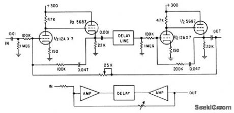
Circuit gives Q of 285 at 500 kc, and is tuned by adjusting delay time. Can be used in any system where high gain, high Q, and stability are needed.-I. F. Barditch, Delay-Line Controls Tuned Amplifier, Electronics, 33:31, p 108. (View)
View full Circuit Diagram | Comments | Reading(645)
| Pages:678/2234 At 20661662663664665666667668669670671672673674675676677678679680Under 20 |
Circuit Categories
power supply circuit
Amplifier Circuit
Basic Circuit
LED and Light Circuit
Sensor Circuit
Signal Processing
Electrical Equipment Circuit
Control Circuit
Remote Control Circuit
A/D-D/A Converter Circuit
Audio Circuit
Measuring and Test Circuit
Communication Circuit
Computer-Related Circuit
555 Circuit
Automotive Circuit
Repairing Circuit