
Circuit Diagram
Index 668
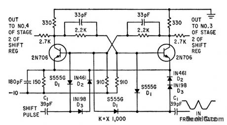
BLOCKING_OSCILLATOR_FOR_SHIFT_REGISTER
Published:2009/7/16 1:42:00 Author:Jessie

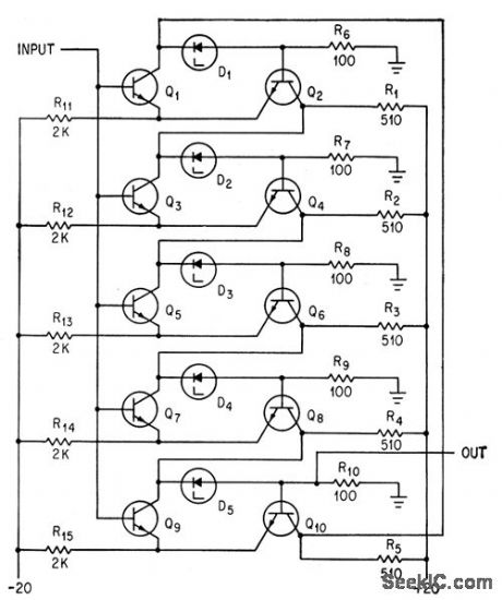
Used to generate series of ten pulses, 20 nsec wide and spaced 40 nsec apart. Each of the ten blocking oscillator stages Q1 is allowed to overshoot and trigger the following stage through an IC coupling network that provides additional delay.-B. K. Ericksen and J. D. Schmidt, Random Pulse Generator Tests Circuits, Encodes Messages, Electronics, 34:25, p 56-59. (View)
View full Circuit Diagram | Comments | Reading(555)
500_MC_BIQUINARY_COUNTER
Published:2009/7/13 23:39:00 Author:May
Quinary divides input events by 5, using current-mode switches, and binary divides quinary output by 2 to give total division of 10.Chief drawback is difficulty of converting to bcd. All transistors ere 2N2708.-R. Englemann, B-Quinary Scaling: Accuracy and Simplicity at 500 Mc, Electronics, 36:46, p34-36. (View)
View full Circuit Diagram | Comments | Reading(1119)
GATE_OUTPUT_INVERTER
Published:2009/7/16 1:42:00 Author:Jessie

Inverter stages compensate for phase inversion of three parallel-transistor nor gates and three series-transistor not and gates.- Transistor Manual, Seventh, Edition, General Electric Co.,1964, p 177. (View)
View full Circuit Diagram | Comments | Reading(599)
SOUND_ACTIVATED_SWITCH
Published:2009/7/13 23:39:00 Author:May

The circuit uses IC1 as a low-noise preamplifier with a voltage gain of 270 times. This is followed by a second stage of amplification, which produces a similar voltage gain. The second stage uses TR1 in the common-emitter mode; this is a conventional arrangement, except for the inclusion of C4. This capacitor provides a considerable amount of high-frequency attenuation, which is necessary in order to prevent instability. Capacitor C5 couples the greatly amplified output of TR1 to a rectifier and smoothing circuit, which gives a positive dc output signal that is roughly proportional to the input-signal level. If the input signal is sufficiently strong, the bias voltage at the gate of VMOS device TR2 will be adequate to bias this transistor into conduction, and the relay that forms its drain load is then activated, A pair of normally open relay contacts are used to control whatever item of equipment is operated by the unit. Of course, the voltage at the gate of TR2 soon decays, as C6 discharges through R8 if the input signal ceases, and the relay is then switched off. The decay time is roughly 1 second, which is about the optimum time for most applications. The attack time of the circuit is only a fraction of a second, and the unit responds almost immediately when a sound is initially picked up by the microphone. (View)
View full Circuit Diagram | Comments | Reading(0)
NEGATIVE_SUPPLY_FROM_A__12_V_SOURC
Published:2009/7/16 1:42:00 Author:Jessie

This switching regulator will produce a -24-V/1.5-A source from a +12-V supply, for applications where a positive-grounded source is necessary. (View)
View full Circuit Diagram | Comments | Reading(624)
1_MC_COMPLEMENTA_RY_TRANSISTOR_COUNTER
Published:2009/7/13 23:38:00 Author:May
Only one stage draws current from power supply, because on stage has both transistors conducting and off stages have both transistors cut off'. Average power drawn is that of single conducting stage and is independent of number of stages. Circuit prefers off state at startup.-Counter Uses Complementary Transistors, Electronic Circuit Design Handbook, Mactier Pub. Corp., N.Y. 1965, p 129. (View)
View full Circuit Diagram | Comments | Reading(885)
__24_V_15_A_SUPPLY_FROM_A___12_V_SOURCE
Published:2009/7/16 1:41:00 Author:Jessie

This switching regulator will produce 1.5 A at 24 V from a 12-V auto battery. It operates as a boost-switching supply using an LT 1070. The diode should be a fast-switching type because this regulator operates above 10 kHz. (View)
View full Circuit Diagram | Comments | Reading(1294)
GATE_GENERATOR_FOR_MISSILE_TRACKER
Published:2009/7/16 1:41:00 Author:Jessie

Position of rectangular gate on tv display is controlled by d-c voltage, while size of gate can be adjusted manually without affecting its center position.-J. R. Kruse, Automatic Tv Tracker Keeps Eye on Missiles, Electronics, 34:13, p 82-87. (View)
View full Circuit Diagram | Comments | Reading(631)
ELECTRONIC_PARROT
Published:2009/7/13 23:36:00 Author:May

This circuit uses a Holtek HT8656 CMOS LSI chip and an 81256 256K X 1 dynamic RAM chip to form a voice record/playback circuit. The sampling rate is either 16 or 32 kbits per second, which allows 8- or 16-second recording time with the 256K DRAM. A 64K DRAM can be used if shorter times are suitable for your application. Power is via a 9-V battery. (View)
View full Circuit Diagram | Comments | Reading(904)
25_A_BATTERY_CHARGER
Published:2009/7/13 23:35:00 Author:May

Battery chargers are usually designed without regard for efficiency, but the heat generated by low-efficiency chargers can present a problem. For those applications, the charger shown in the figure delivers 2.5 A with efficiency as high as 96 percent. It can charge a battery of one to six cells while operating from a car battery. IC1 is a buck-mode switching regulator that controls the external power switch, Q1, and the synchronous rectifier. IC1 includes a charge pump for generating the positive gate-drive voltage required by Q1. The battery-charging current develops a voltage across the 25-MΩ resistor (R3) that is amplified by the op amp and presented as positive-voltage feedback to IC1. This feedback enables the chip to maintain the charging current at 2.5 A. While charging, the circuit can also supply current to a separate load, up to a limit set by current-sense transformer T1 and sense resistor R1. T1 improves efficiency by lowering power dissipation in R1. The transformer turns ratio (1:70) routes only 1/70 of the total battery-plus-load current through R1, creating a feed-back voltage that enables IC1 to limit the overall current to a level compatible with the external components. (View)
View full Circuit Diagram | Comments | Reading(1458)
CAPACITOR_CHECKER
Published:2009/7/16 1:39:00 Author:Jessie
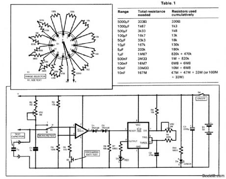
The circuit for the capacitor checker is shown in the figure. Switch S2 is used to select the Mea-sure (M) or Test (T) mode, as required. Assume for the moment that it is in the M position, as shown. Operational amplifier IC1 is configured as a voltage comparator. The values of the resistors have been chosen to provide 86 percent (actually, it is nearer 87 percent) of the supply voltage to the noninverting input, pin 3. Meanwhile, the capacitor being measured, Ct, charges through resistor R1, so the voltage across it rises and follows the form shown in Fig. 2.R1 is selected from a chain of resistors using the rotary range switch, S1 (inset). The value of R1 in the chain will be such that with a capacitor at the top of the range selected (e.g.a100-nF capacitor on the 100-nF range), the time constant will be 1.66 s. The values of R1, required to provide this time constant on the various ranges are shown in Table 1. Assuming that the test capacitor Ct is discharged to begin with, after two time constants have elapsed, the voltage across the capacitor will rise above 86 percent of the supply. The op amp switches off, with pin 6 becoming low. While IC1 pin 6 is high (during the initial stages of C, charging), IC2 pin 4 is maintained in a high state, which enables the IC. When the capacitor charges through two time constants, IC1 pin 6 becomes low, IC2 is disabled, and the flashing stops. The nominally low state of IC1 output would still be high enough to enable IC2 if connected directly, and the two diodes (D1 and D2) correct this. Resistor R6 maintains IC2 pin 4 low in the absence of a high state from IC1 output. The rate at which pulses are produced depends on the values of fixed resistors R8 and R9 and preset potentiometer VR2, in conjunction with capacitor C2. With the values chosen, they will be delivered at between 1 and 10 per second approximately, depending on the adjustment of VR2. VR2 will be adjusted so that exactly three flashes per second are provided. Ten flashes, therefore, correspond to 3.33 s, which is equal to two time constants for a capacitor at the limit of the range selected. (View)
View full Circuit Diagram | Comments | Reading(1820)
2_METER_SCANNER
Published:2009/7/13 23:35:00 Author:May
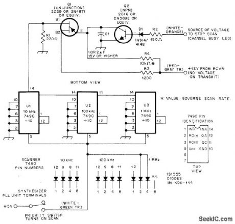
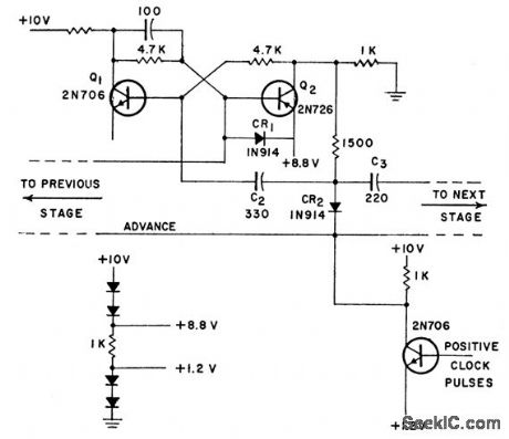
Designed for use with KDK-144 amateur 2-meter transceiver to provide automatic scanning between 146 and 147.990 MHz. When transceiver is switched to priority position, +5 VDC is applied to 7490 decade counters U1, U2, and U3 to activate scanner. Scanning stops when signal strong enough to open squelch turns on Darlington-connected transistors a1 and Q2, shorting UJT timing capacitor C1 which is 1-2 μF.-R. W. Shoemaker, Jr., A Scanner for KDK, QST, 0ct. 1978, p 36-37. (View)
View full Circuit Diagram | Comments | Reading(868)
DECADE_SCALER
Published:2009/7/13 23:34:00 Author:May
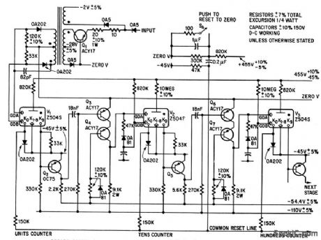
For accurate timing applications up to 400 pps.-G. Jeynes, Using Cold.-Cathode Tubes to Count and Store, Electronics. 38:8, p 80-89. (View)
View full Circuit Diagram | Comments | Reading(539)
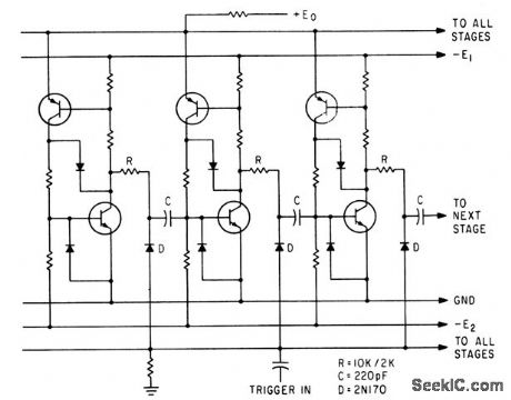
HIGH_SPEED_FLIP_FLOP
Published:2009/7/16 1:39:00 Author:Jessie
Used in producing complex pulse sequences up to 4 billion bits in length. Drives n-stage shift generator that provides modulo-2 additions.-B. K. Ericksen and J. D Schmidt, Random Pulse Generator Tests Circuits, Encodes Messages, Electronics, 34:25, p 56-59. (View)
View full Circuit Diagram | Comments | Reading(559)
7625_AND_816_MHz
Published:2009/7/13 23:33:00 Author:May

MCl0102 ECL quad NOR gate provides convenient switching between two crystal oscillators, as required for change from receive to transmit in transceiver. Output level of about 0.8 V P-P can easily drive 50-ohm load and is fully buffered from oscillator sections. Gate A provides bias for oscillator gates B and C. Use 270 ohms for R1-R3, Crystals are fifth overtone; YB is 81.6 MHz with 97 nH for LB and 39 pF for CB, and YC is 76.25 MHz with 104 nH for LC and 39 pF for CC.-G. Griesmyer, Clocked CMOS One-Shot Has No RC Time Constant, EDN Magazine, May 20, 1978, p 164 and 172.
(View)
View full Circuit Diagram | Comments | Reading(976)
GAS_TUBE_RING_COUNTER
Published:2009/7/13 23:33:00 Author:May
Uses Philips trigger tubes in decade counter having maximum speed of 2,500 pps Bias developed at cathode is fed through G to prime following stage Readout display can be Burroughs Nixie HBl06 or other numerical indicator.-P. G. Hodgson, Cold-Cathode Ring-Counter Drives Numerical Indicator, Electronics, 33:14, p 80. (View)
View full Circuit Diagram | Comments | Reading(806)
REVERSIBLE_TEN_SIAGE_RING_COUNTER
Published:2009/7/13 23:32:00 Author:May
Can be operated above 100 kc. Reversible operation requires binary control, such as by bistable mvbr, to determine direction. Upper transistors are 2N414 and lower are 2N488.Other resistors are 1K.-N. C. Hekimian, PNP-NPN CIRCUITS: New Look at a Familiar Connection, Electronics, 35:47, p 42-46. (View)
View full Circuit Diagram | Comments | Reading(904)
CRICKET_CHIRP_SIMULATOR
Published:2009/7/13 23:32:00 Author:May

Power is supplied from a 9-V battery, B1; current drain is a little under 2 mA, so an alkaline battery should last more than 250 hours. Switch S1, the power switch, is a part of potentiometer R10, which also acts as a volume control. A duty cycle is generated by op amp U1-a, which is configured as a pulse generator. Diode D1 establishes a fast charging rate that generates a 0.22-second period, which matches the duration of a cricket's seven-beat chirp. The discharge rate is established by R2 to generate a reset time of 0.35 second. One half of an ICM7556 CMOS timer, U2-a, is used to simulate the amplitude modulation of a chirp. Timer U2-b is configured as a conventional pulse generator with a symmetrical duty cycle and an output frequency of 2 kHz. The output of U2-b is used to switch Q2 on and off, which produces a voltage across volume control R10 that has the magnitude of the instantaneous voltage across C2 with a 2-kHz sampling rate. A portion of that voltage is applied to U1-b, which is configured as a unity-gain, noninverting buffer that drives the piezo element. (View)
View full Circuit Diagram | Comments | Reading(826)
REMOTE_TUNING
Published:2009/7/13 23:32:00 Author:May
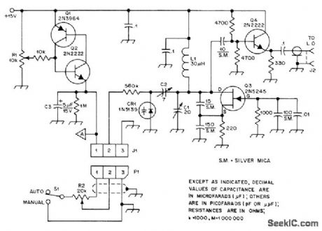
Simple sweep generator and 5-5.5 MHz VCO provide remote manual or automatic electronic tuning of 6-meter transceiver, for quick check of possible band openings a few kilohertz from frequency to which receiver is normally tuned. To adjust, set S1 on MANUAL and turn R2 fully counterclockwise. If signal at lowest received frequency is applied to antenna jack, signal can be centered within IF passband of receiver by adjusting C1. Next, turn R2 fully clockwise, apply signal at highest frequency to be received, and center signal within passband again by adjusting C2. With S1 in AUTO position, R1 determines highest frequency tuned. If sweep rate is too low, reduce value of C3. Point A is used to drive CRO through FET buffer stage, for displaying signals present within sweep range as pips on screen.-J. R. Bingham, Sweep 6 Meters and Really Clean Up! QST, April 1977, p 27-28. (View)
View full Circuit Diagram | Comments | Reading(1437)
TIMED_NiCd_CHARGER
Published:2009/7/13 23:29:00 Author:May

The primary supply is provided by 230 V through transformer T1, diodes D1 and D2, and reservoir capacitor C2. A supply for the timing circuit is provided through diode D3, with resistor R1 and zener diode D4 to keep it to a safe voltage for the CMOS devices used. These CMOS devices, IC1 and IC2, use so little current that the timer will keep going for up to 30 s if the power fails, preventing the charge period from being restarted by every minor glitch in the supply. IC1 is a 4060B 14-stage divider with built-in oscillator. Pressing switch S1 sets all its outputs low, so diode D5 is reverse-biased and the oscillator operates. With the component values shown, it runs at about 0.17 Hz, so the last output of the divider, pin 3, goes high after about 14 h. This applies forward bias to D5, which stops the oscillator. The first timer of the 7556 dual CMOS timer IC2 is connected to operate as an oscillator with a frequency of about 0.5 Hz with a duty cycle of about one to five. Pin 4 is an active low reset for this timer, so although the input to this from IC1 is low, its output is also low. The second timer is used as an inverter to convert this to a high output, which, via resistor R8, activates the output constant-current generator. When IC1 times out, the oscillator in IC2 starts running, and the current generator is then pulsed for about 400 ms every 2 s. NiCds have quite a high self-discharge rate: about 10 percent of capacity per week. If left on this charger, they will be kept fully topped up ready for use without overcharging, and by flashing in time with the current pulses, LED D10 will let the user know that the main charge period is complete
(View)
View full Circuit Diagram | Comments | Reading(870)
| Pages:668/2234 At 20661662663664665666667668669670671672673674675676677678679680Under 20 |
Circuit Categories
power supply circuit
Amplifier Circuit
Basic Circuit
LED and Light Circuit
Sensor Circuit
Signal Processing
Electrical Equipment Circuit
Control Circuit
Remote Control Circuit
A/D-D/A Converter Circuit
Audio Circuit
Measuring and Test Circuit
Communication Circuit
Computer-Related Circuit
555 Circuit
Automotive Circuit
Repairing Circuit