
Circuit Diagram
Index 660
ZERO_CROSSING_HIGH_POWER
Published:2009/7/14 2:07:00 Author:May

AC relay uses MFC8070 zero-voltage switch to provide gate current pulses for triac under control of differential input voltages derived from output of 4N28 optoisolator. When LED is off, voltage at pins 1 and 2 of switch is positive with respect to pin 3, inhibiting switch so no current pulses go to mac gate. When LED is energized by logic input, gate current pulses are generated at zero-voltage excursions of AC power source. Transistor ensures adequate gate drive at low temperatures. For normally-on configuration,interchange input connections 3 and 1-2 of switch. Triac can be selected to handle resistive loads from 4 to 40 A.-T. Mazur, Solid-State Relays Offet New Solutions to Many Old Problems, EDN Magazine, Nov. 20, 1973, p 26-32. (View)
View full Circuit Diagram | Comments | Reading(2191)
RING_COUNTER_WITH_VISUAL_READOUT
Published:2009/7/14 2:07:00 Author:May

Uses only six components per stage. Combining of counter and indicator functions gives low battery drain. After reset button is re leased, 0.22-mid capacitor insures that first stage turns on. Current is drown by stage only when lamp is on. Any number of stages may be included in ring.- Transistor Manual, Seventh Edition, General Electric Co., 1964, p 203. (View)
View full Circuit Diagram | Comments | Reading(769)
1_kW_GROUNDED_GRID
Published:2009/7/14 2:07:00 Author:May

Class B linear amplifier for amateur transmitter can be switched to any band from 80 through 10 meters Do not exceed 200-mA grid drive, and do not apply full excitation without plate voltage. Tube requires blower for air cooling. Article covers construction and adjustment. -E, Hartz, 4-1000 A Grounded Grid Linear, 73 Magazine,July 1974, p 17, 19-20,22-24, and 26.
(View)
View full Circuit Diagram | Comments | Reading(2545)
PIN_DIODE_HIGH_SOLATION_SWITCH_CIRCUIT
Published:2009/7/14 2:07:00 Author:May

This circuit is a basic PIN-diode switch using series- and shunt-diode building blocks. R is chosen from Idiode=(Vcc-Vdiode)/R, where Idiode is the specified diode current and R is total dc circuit resistance. (View)
View full Circuit Diagram | Comments | Reading(676)
450_470_MHz_AT_10_W
Published:2009/7/14 2:06:00 Author:May

Power amplifier for land-mobile 12.5-V transmitter is constructed on double-sided microstrip substrate, Power gain at 470 MHz is 14.5 dB, and overall efficiency is 55%,-G. Young, UHF Microstrip Amplifiers Utilizing G-10 Epoxy-Glass Laminate, Motorola, Phoenix, AZ, 1976, AN-578, p 3. (View)
View full Circuit Diagram | Comments | Reading(777)
SWITCHING_4500_W_BELOW_5_kHz
Published:2009/7/14 2:05:00 Author:May

Simple Darlington connection of Delco DTS-709 transistors serves for switching of uρ to 700 V at 7A for low-speed motor control,regulator,and inverter applications.-″Low cost 'Dualithic Darlington'Switches 4500 Watts at up to 10 kHz,″ Deleo, Kokomo, IN, 1973, Application Note 54,p 3.
(View)
View full Circuit Diagram | Comments | Reading(1281)
BATTERY_IMPEDANCE_MEASURER
Published:2009/7/14 2:05:00 Author:May

By applying an ac voltage superimposed on a ten times larger negative dc voltage (at VFG), the function generator determines the battery current drawn by Q1 (see the figure). The generator voltage causes the op-amp (IC2) output to go high and turn Q1 on, which allows battery current to flow through the high-side current-sensing amplifier (IC1). The output current of IC1, on pin 8, is equal to 1/2000 of this battery current. As a result, IC1, IC2, and Q1 form a loop in which the op amp forces a virtual ground at the IC1/IC2 end of R3. The op amp's extremely low-voltage offset (10 μV maximum) ensures accuracy. This virtual-ground condition enables the voltage divider (R5, and R3 in parallel with R4) and the function generator to determine the voltage across R3. The resulting current in R3 is iR3 = RP X VFG/【(RP+R5)R3】, where RP is the parallel combination of R3 and R4. Substituting resistor values and noting that battery current (iB) is 2000 times iR3,iB=-VFG/5.To operate the circuit, set the function generator's ac voltage to approximately 10 percent of its dc component. The equation then gives the resulting ac current in the battery (iB). Using an ac voltmeter, you can measure the ac voltage across the battery (vB) and calculate the average cell impedance as vB/NiB, where N is the number of cells. The circuit easily accommodates battery voltages of 3 V or more. (View)
View full Circuit Diagram | Comments | Reading(754)
1_MC_COUNTER
Published:2009/7/14 2:04:00 Author:May
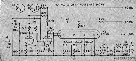
Increasing counting speed to this value requires special hydrogen gas in counter tubes and reduction of tube capacitances. Monostable mvbr V1-V2 is triggered by 5-V negatiye pulses. Cathode resistors of V3 ore bridged by capacitors to reduce effects of capacitive coupling between main and auxiliary cathodes.-K. Apel and P. Berweger, Miniature Gas-Filled Tubes For High-Speed Counting, Electronics, 33:8, p 46-47. (View)
View full Circuit Diagram | Comments | Reading(855)
RELAY_DRIVE
Published:2009/7/14 2:04:00 Author:May

Logic input of 0 turns first transistor off, allowing base of next transistor to go high so it turns on and energizes relay for achieving desired control function.-D, D. Mickle, Practical Computer Projects, 73 Magazine, Jan. 1978, p 92-93. (View)
View full Circuit Diagram | Comments | Reading(728)
SERIES_SHUNT_PIN_DIODE_RF_SWITCH
Published:2009/7/14 2:03:00 Author:May

A combination of series and shunt switching results in superior isolation between the input and output when in the OFF condition. Diodes can be MV3404 or similar types. (View)
View full Circuit Diagram | Comments | Reading(0)
LOW_POWER_RING_COUNTER
Published:2009/7/14 2:02:00 Author:May
Requires only 6 mw at 1.5V. Reset pulse turns on first stage with its trailing edge.- Transistor Manual, Seventh Edition, General Electric Co, 1964, p 431 (View)
View full Circuit Diagram | Comments | Reading(860)
GEIGER_COUNTER_TO_IBM_INTERFACE
Published:2009/7/14 2:01:00 Author:May

The simplest way to connect a Geiger counter to the IBM computer is to use a headphone jack to the parallel port. The headphone jack provides a +5- to 0-V pulse for each radioactive particle detected. The signal from the Geiger counter is +5 V. When radiation is detected, the signal pulses down to 0 V for a few milliseconds before returning to +5 V. Even though the signal is in the 0- to +5-V range, it is not safe to connect wires from an external circuit or instrument directly to the parallel-port lines without buffering. The op amp operates from a single-pole +5-V power supply. In this particular case, invert the signal from the Geiger counter. Because the pulse signals are +5 to 0 V, we do not require any amplification from our op amp. Therefore, the op arnp is configured as an inverting unity-gain follower. Remember that the Geiger counter outputs a steady +5V through the headphone jack. When it detects radiation, the output pulses down to 0 V for a few milliseconds. By inverting the Geiger counter signal with the op amp, the computer reads a steady 0 V on its line and a +5-V pulse when radiation is detected.
(View)
View full Circuit Diagram | Comments | Reading(1381)
VHF_TRANSCEIVER_T_R_SWITCH
Published:2009/7/14 2:01:00 Author:May

This is a transceiver transmit/receive switch that uses a PIN diode instead of a relay. Diodes can be MV3404 or similar types. (View)
View full Circuit Diagram | Comments | Reading(656)
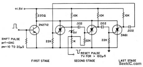
VARIABLE_TIMING_RING_COUNTER
Published:2009/7/14 2:01:00 Author:May
Shift pulses are generated by unijunction transistors, with interval between pulses deter. mined by CT and RT. RT can have different value for each stage of Gaunter, as shown.- Transistor Manual, Seventh Edition, General Electric Co. 1964, p 430. (View)
View full Circuit Diagram | Comments | Reading(803)
1200_W_PEP_POWER_AMPLIFIER
Published:2009/7/14 2:00:00 Author:May

Ceramic tetrodes are operated as low-mu triodes, with control grids tied to cathodes. Amplifier takes about 200-W drive. Tuned-cathode input circuit presents better load to exciter. Bias is developed through 33K cathode resistor that is shorted out by relay during operation. In standby mode, plate current is virtually zero. Article covers construction and operation, with emphasis on proper cooling of tubes. Separate tuned circuits are required for each amateur band. L1 and L2 are 0.15 μH, L3 and L4 are 0.31 μH, and L5 is 1.3 μH. PC-1 and PC-2 are 3 turns No. 16 enamel wound on 50-ohm 2-W carbon resistor-S. W. Hochman, The Ample Amplifier, 73Magazine, March 1973, p 50-54. (View)
View full Circuit Diagram | Comments | Reading(7149)
BASIC_PIN_DIODE_RF_SWITCH
Published:2009/7/14 1:59:00 Author:May

D1 is a pin diode (MV3404) used as a SWitch,with dc bias supplied via R1. L1 and L2 are RF chokes An alternative approach eliminating the RF chokes is also shown (View)
View full Circuit Diagram | Comments | Reading(1005)
DECIMAL_CODED_COUNTER
Published:2009/7/14 1:59:00 Author:May
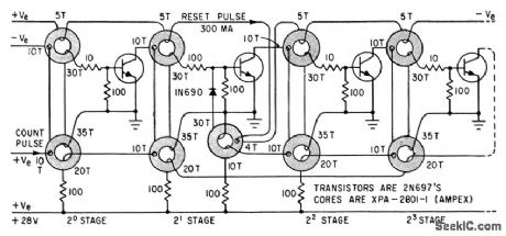
Addition of one core and one diode per decade converts straight-binary counter to decimal-coded counter.-W. R. Johnston, Multiaperture-Core Counters Give Nondestructive Storage Readout, Electronics, 34:24, p 62-64. (View)
View full Circuit Diagram | Comments | Reading(982)
VMOS_5_W_BROADBAND
Published:2009/7/14 1:59:00 Author:May

Single-transistor broadband linear amplifier uses Siliconix VMP1 to provide 15-dB gain over entire frequency range of 2 to 100 MHz.-G. D. Frey VMOS Power Amplifiers-This Broadband Circuit Outputs 8W with a 15 dB Gain, EDN Magazine. Sept 5, 1977, p83-85.
(View)
View full Circuit Diagram | Comments | Reading(808)
10_W_AT_450_MHz
Published:2009/7/14 1:56:00 Author:May

Uses Motorola MHW-710 sealed power module drawing 2.7 A on 13.8 VDC. Developed for use with fast-scan amateur TV transmitter having audio on video carrier and TR switching. Relay K1 is Archer (Radio Shack) 275-206. L1 is Ferroxcube VK200-201 4B.-B. J. Brown, Super Simple 450 MHz Rig, 73Magazine, Aug. 1976, p 72-75. (View)
View full Circuit Diagram | Comments | Reading(1131)
SHUNT_PIN_DIODE_RF_SWITCH
Published:2009/7/14 1:56:00 Author:May

D1 is a PIN diode (MV3404) used as a switch, with dc bias supplied via R1 and L1.This shunt PIN-diode switching circuit directs signals to ground when D1 is forward-biased. (View)
View full Circuit Diagram | Comments | Reading(1205)
| Pages:660/2234 At 20641642643644645646647648649650651652653654655656657658659660Under 20 |
Circuit Categories
power supply circuit
Amplifier Circuit
Basic Circuit
LED and Light Circuit
Sensor Circuit
Signal Processing
Electrical Equipment Circuit
Control Circuit
Remote Control Circuit
A/D-D/A Converter Circuit
Audio Circuit
Measuring and Test Circuit
Communication Circuit
Computer-Related Circuit
555 Circuit
Automotive Circuit
Repairing Circuit