
Circuit Diagram
Index 655
HIGH_TRIGGERING_SENSITIVITY
Published:2009/7/15 22:20:00 Author:Jessie

Semiconductor diode is used as series nonlinear element in feedback loop of monostable mvbr, to give good stability along with improved triggering sensitivity for nuclear event registration, pulse analysis, counting, and time modulation.-M.M. Voiinovic, Series Diode Increase Multivibrator Sensitivity, Electronics, 32:17, p 90-91. (View)
View full Circuit Diagram | Comments | Reading(722)
DARL_ALARM
Published:2009/7/15 22:20:00 Author:Jessie

This alarm senses darkness. Photocell PCC1 is normally irradiated with light and has a low resistance. In darkness, the resistance increases, and enough bias is available to turn on Tr1, activating the oscillator circuit consisting of IC1 and associated components. This produces a tone in speaker LS1. (View)
View full Circuit Diagram | Comments | Reading(866)
OPAMP_AS_MILLIVOLT_REFERENCE_1
Published:2009/7/15 22:20:00 Author:Jessie

High-performance bipolar-input Precision Monolithics OP-05CJ instrumentation opamp is connected as unity-gain buffer. Output is adjusted to desired reference voltage with pot connected to offset nulling terminals. Reference range is -3.5 mV to +3.5 mV, and long-term drift of zener less source is less than 3.5 μV per month.-D. Soderquist, Simple Precision Millivolt Reference Uses No Zeners, Precision Monolithics, Santa Clara, CA, 1975, AN-10. (View)
View full Circuit Diagram | Comments | Reading(1372)
2_Hz_TO_1_MHz
Published:2009/7/15 22:19:00 Author:Jessie

General-purpose laboratory pulse generator uses four CD4047A MVBRs to provide six overlapping ranges of frequencies along with pulse-width control, delayed sync, and gating from high-level or low-level input. When delay switch is IN, MVBR at upper center produces variable output delay from 1.5 μs to 250 ms with respect to sync pulse. When delay pulse is OUT, this mono MVBR is bypassed and inherent delay is then about 400 ns. Signal output is buffered with CD4041A for driving any required load. Supply voltage is not critical and can be taken from device under test.- COS/ MOS Integrated Circuits, RCA Solid State Division, Somerville, NJ, 1977, p 619-620. (View)
View full Circuit Diagram | Comments | Reading(1765)
SUMMING_AND_WEIGHTING_NETWORK
Published:2009/7/14 2:38:00 Author:May

Consists of eight identical circuits. Precise value of direct current from constant-current source, fed into first node of resistive ladder network, produces 2.5-v step at summing and weighting network output, or half of maximum analog input of 5 v.-W.B. Towles, Transistorized Analog-Digital Converter, Electronics, 31:31, p 90-93. (View)
View full Circuit Diagram | Comments | Reading(659)
OPAMP_AS_MILLIVOLT_REFERENCE
Published:2009/7/15 22:19:00 Author:Jessie

R4 at input of voltage-foilower opamp permits varying ref erence voltage from 0 up to limit of zener. A2 compensates for loading of zener by R4. Dual opamp cannot be used because negative supply terminal of A2, must be slightly more negative than -3 V common to permit linear output operation down to 0 V. If additional load current is required, NPN booster transistor can be used with A2.-W. G. Jung, IC Op-Amp Cookbook, Howard VV, Sams, Indianapolis, IN, 1974, p 155-157. (View)
View full Circuit Diagram | Comments | Reading(1238)
MEMORY_REFRESHER
Published:2009/7/15 22:17:00 Author:Jessie

Delivers high-energy pulses in extremely low duty-cycle mode. Developed to provide memory-refresh pulses for MOS memory system from standby battery. Circuit is basically programmable UJT oscillator with divider R2-R3 setting threshold or trigger level. To complete one cycle and start next, UJT is turned off by zener. Current through L1 drops, and resulting negative transient at base of Darlington outs it off. This generates high-power pulse with very sharp rise and fall times. Charging sequence then starts again to give sustained oscillation. Article gives design equations.-J. P. Stein, PUT Delivers Ultra-Low-Power. High-Energy Pulses, EDN Magazine, Sept.1, 1972, p 51-52. (View)
View full Circuit Diagram | Comments | Reading(1251)
BCD_CONTROL_OF_GAIN
Published:2009/7/14 2:38:00 Author:May


Provides optically coupled input and BCD-selected attenuation factor, for combination with fixed-gain DC amplifier to give programmable gain capability. Output of A-8402 V/F converter feeds programmable modulo-n decade counter chain through optoisolator, to give frequency division by BCD factor applied to selector inputs. 74122 retriggerable mono MVBR makes duty cycle of counter output compatible with requirements of second converter connected to give output voltage that is scaled reproduction of input voltage. Circuit performance is comparable to that of high-cost instrumentation amplifier.-K. W. Kissinger, Low-Cost Isolation Amp Provides BCD-Selectable Gain, EDN Magazine, Oct. 20, 1977, p 82-83. (View)
View full Circuit Diagram | Comments | Reading(628)
10000_V_WITH_ZENER
Published:2009/7/15 22:17:00 Author:Jessie

Circuit provides stable current biasing of zener and adjustable output voltage by bootstrapping excitation current off output voltage. Commercial version of circuit (Analog Devices AD2700) achieves temperature drift of only 3 PPM/℃.-J. Williams, Don't Bypass the Voltage Reference That Best Suits Your Needs, EDN Magazine, 0ct. 5, 1977, p 53-57. (View)
View full Circuit Diagram | Comments | Reading(755)
ANALOG_DIFFERENTIAL_AMPLIFIER
Published:2009/7/14 2:36:00 Author:May
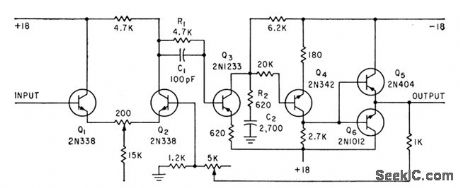
Input impedance is above 300,000 ohms and output impedance 1 ohm, in d-c amplifier for analog input channel.Q3 and Q4 provide gain and phase inversion for feedback through complementary emitter-follower Q5-Q6 to differential amplifier Q1-Q2.-N. Aron and C.Granger, Analog-To-Digital Converter Uses Transfluxors, Electronics,35:20, p 62-66. (View)
View full Circuit Diagram | Comments | Reading(669)
AUDIO_CONTROLLED_LAMP_DIMMER
Published:2009/7/15 22:17:00 Author:Jessie

The audio input to J1 lights low-voltage lamp I1. This light illuminates light-dependent resistor R3 (100 KΩ to 1 MΩ dark resistance) and modulates the intensity of the lamp plugged into SO1. L1 and C1 suppress RFI caused by the triac phase-control circuit. D1 and TR1 are a diac and a triac, respectively, and are the types used in common lamp dimmers. (View)
View full Circuit Diagram | Comments | Reading(1051)
5_V_FROM_15_V
Published:2009/7/15 22:16:00 Author:Jessie

Used as reference for A/D converter when reference voltage required is below that of zener, permitting simplified circuit design. Zener drift contributes proportionally to output temperature drift, while opamp offset drift contributes at greater rate. Opamp is unnecessary if high output impedance can be tolerated.-R. C. Dobkin, Don't Forget Reference Stability When Designing A-to-D Converters, EDN Magazine, June 20, 1977, p 105-108. (View)
View full Circuit Diagram | Comments | Reading(719)
TELEPHONE_BUG
Published:2009/7/14 2:35:00 Author:May

Q1 is an oscillator tuned to a quiet spot in the FM broadcast band. Dc from the line powers the bug. Diodes D1 through D4 ensure proper polarity. R1 maintains a suitable voltage drop for the bug. Audio on the line causes incidental FM, which can be heard on an FM receiver tuned to the frequency of the oscillator.Warning: Use of this device for certain purposes could violate federal and/or state laws and subject the violator to prosecution. (View)
View full Circuit Diagram | Comments | Reading(683)
DELAYED_PULSE
Published:2009/7/15 22:15:00 Author:Jessie

Both time and duration of output pulse are programmable by selection of RC networks. Original and delayed clock pulses can both be used in gating circuits. With values shown, output pulse is 1 ms wide and is delayed 15 μs from trailing edge of clock pulse.-D. T. Anderson, Operational Amplifier Makes a Simple Delayed Pulse Generator, EDN Magazine, July 1, 1972, p 55. (View)
View full Circuit Diagram | Comments | Reading(686)
_15_V_HIGH_PRECISION
Published:2009/7/15 22:15:00 Author:Jessie


Uses 725 opamp having low offset drift and high common-mode rejection in combination with low-drift version of 1N4611 zener to give highly stable operation at output currents up to 100 mA. Close-tolerance low-temperature-coefficient film or wirewound resistors are required for R1, R2, and R3. Remote sensing at load corrects for wiring voltage drops.-W. G. Jung, IC Op-Amp Cookbook, Howard W. Sams, Indianapolis, IN, 1974, p 152-155. (View)
View full Circuit Diagram | Comments | Reading(633)
HYSTERESIS_STABILIZING_LIGHT_SENSOR
Published:2009/7/15 22:14:00 Author:Jessie
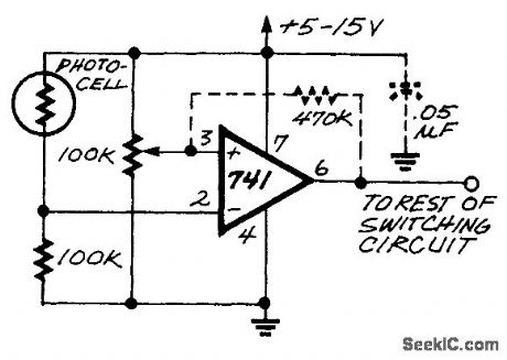
This light turn-on circuit originally had oscillation problems. The 470-kΩ resistor introduces the hysteresis to prevent the oscillation. You can experiment with the value of the resistor for best results in your application. (View)
View full Circuit Diagram | Comments | Reading(1132)
TIMER_COUNTER
Published:2009/7/14 2:34:00 Author:May

Basic circuit using XR2240 programmable timer/counter acts as programmable mono when S1 is closed, with output pulse width being a multiple in binary of RC seconds. With 8-bit binary counter, time delays range from 1 RC to 255 RC seconds. As an exi ample, if only pin 6 (dividing input frequency by 32) is connected to common output bus, duration of output pulse will be 32 RC seconds. Similarly, with pins 1, 2, 5, and 7 connected to bus, delay is 83 RC seconds. With S1 open for astable operation, output frequency is 1/t hertz where t is multiple of RC from 1 to 255. VCC is 4-15 V. - H. M. Berlin, IC Timer Review, 73 Magazine, Jan. 1978, p 40-45. (View)
View full Circuit Diagram | Comments | Reading(2972)
INTERLACED_SYNC
Published:2009/7/15 22:14:00 Author:Jessie

Uses Sylvania 15-37701-1 IC made by Texas Instruments for 1974 Sylvania color TVs, where it serves to generate sync signals whenever off-the-air sync is temporarily Lost. IC has divide-by-2, divide-by-25, and mono MVBR stages. Used in circuit shown to provide interlaced sync for black and white amateur TV camera, Required 31.5-kHz input is obtained from 6300-kHz crystal oscillator and three flip-flops that divide by 200 With 74121 mono and 7400 gate connected as shown, interlaced sync outputs are obtained.-R. Suding, Master Sync Generator, 73 Magazine, July 1975, p 96. (View)
View full Circuit Diagram | Comments | Reading(1203)
33_OR_5_V_ANALOG_SWITCHES
Published:2009/7/14 2:33:00 Author:May

By adding a single component to a 3-V only or 5-V only board,you can operate conventional CMOS analog switches with Performance approaching that specified with ±15-V Supplies, This means fast switching,low ON resistance,CMOS /TTL compatibility, low power consumption,and a signal range (±Vcc) that exceeds the input supply range (Vcc to ground).Simply add a charge-ump voltage converter:(IC1),which produces±2-Vcc outputs from a Vcc input .These unregulated voltages ensure reliable switch operation for Vcc levels as low as 3 V. Logic thresholds for the switch remain unaffected A Vcc of 3 V (for instance)produces,±6 v rails for the switch (IC2),resulting in ON resistance<30Ω,switching times<200 ns,leakage<0.1 nA,and Vcc ourrent<0.5mA Raising Vcc to 5 V produces±10-V rails,resulting in ON resistance<20Ω,switching times<150 ns,leakage<0.4 nA,and Vcc current<l.3 mA IC1 can easily power additional switches and/or low-power Op amps,but more than a few milliamperes of load current degrades Performance by lowering the unregulated supply rails.
(View)
View full Circuit Diagram | Comments | Reading(758)
1_W_ON_175_kHz
Published:2009/7/14 2:32:00 Author:May

Simple one-tube circuit with zener-regulated power supply provides amateur CW operation in30-kHz segment of long wave (VLF) spectrum Adjust L1 and L2 to resonance with crystal used, then adjust coupling between them until meter between plate and ground reads correct current for legal limit of 1-W power input to final stage. Antenna is vertical mast insulated from ground, with transmitter directly at its base,-J. V. Hagan, A Crystal-Con-trolled Converter and Simple Transmitter for 1750-Meter Operation,QST, Jan. 1974, p 19-22. (View)
View full Circuit Diagram | Comments | Reading(752)
| Pages:655/2234 At 20641642643644645646647648649650651652653654655656657658659660Under 20 |
Circuit Categories
power supply circuit
Amplifier Circuit
Basic Circuit
LED and Light Circuit
Sensor Circuit
Signal Processing
Electrical Equipment Circuit
Control Circuit
Remote Control Circuit
A/D-D/A Converter Circuit
Audio Circuit
Measuring and Test Circuit
Communication Circuit
Computer-Related Circuit
555 Circuit
Automotive Circuit
Repairing Circuit