
Circuit Diagram
Index 656
50_WPUSH_PULL
Published:2009/7/14 2:30:00 Author:May

Single RF power amplifier stage uses broadband transmission-line transformers, operates between 50-ohm source and load impedances, and produces 50 W peak envelope power from 28-V supply over band of 2-30 MHz. Article gives design equations for toroid transformers.-W. P .Reilly, Transmitter Power Amplifier Design, Wireless world, Sept1975, p 417-422. (View)
View full Circuit Diagram | Comments | Reading(1017)
TWO_CAMERA_VIDEO_SWITCH
Published:2009/7/15 22:12:00 Author:Jessie

DG200 CMOS switches with built-in drivers provide 94-dB isolation at 10 MHz between on and off cameras. Desired camera is turned on by applying low logic level to select line for that camera.- Analog Switches and Their Applications, Siliconix, Santa Clara, CA, 1976, p 7-26. (View)
View full Circuit Diagram | Comments | Reading(1005)
PREFERRED_MONOSTABLE
Published:2009/7/15 22:12:00 Author:Jessie

Generates positive or negative rectangular gate in response to positive input trigger. Duration of gate will remain within 5% of initial preset value, and amplitude will be constant within 30%. Circuit is self-timing, with output gate duration determined by configuration and values of R3, R4, and C3. Used in radar to establish period during which main display sweep is presented, to provide crt unblanking gate, and to provide enabling gate for distance mark generator.-NBS, Handbook Preferred Circuits Navy Aeronautical Electronic Equipment, Vol. I, Electron Tube Circuits, 1963, PC 41, p 41-2. (View)
View full Circuit Diagram | Comments | Reading(687)
RF_MODULATOR
Published:2009/7/15 22:11:00 Author:Jessie

First section of free-running 7413 Schmitt-trigger oscillator runs at one-third of desired TV-channel carrier frequency (about 20 MHz for channel3) and drives buffer section whose output is square wave at oscillator fundamental. Q1 modulates RF output by varying effective supply voltage to IC. Since standard video is 1 V P-P, modulation depth is about 20% with 5-V supply. Capacitive connection is made to TV set, using short lengths of 300-ohm line after removing regular antenna leads from set used as experimental display terminal for microprocessor. R1 determines frequency of oscillation; ad just for best reception.-W, Banks, The Waterloo RF Modulator, BYTE, Jan. 1978, p94. (View)
View full Circuit Diagram | Comments | Reading(0)
101_V_STANDARD_CELL_REPLACEMENT
Published:2009/7/15 22:11:00 Author:Jessie

National LM199 temperature-stabilized 6.95-V reference is applied to LM3308 opamp through LM321 preamp to give standard-cell replacement that can be adjusted to output of exactly 1.01 V. Null offset of opamp before adjusting for proper output voltage, - Linear Applications, vol. 2, National Semiconductor, Santa Clara, CA, 1976, AN-161, p 5. (View)
View full Circuit Diagram | Comments | Reading(790)
±25_V
Published:2009/7/15 22:11:00 Author:Jessie

Precision Monolhhics REF-02 voltage reference and OP-02 inverting opamp provide desired references when used with supply volt-ages shown.- +5 V Precision Voltage Reference/Thermometer, Precision Monolithics, Santa Clara, CA, 1978, REF-02, p 6. (View)
View full Circuit Diagram | Comments | Reading(732)
HORIZONTAL_SYSTEM_FOR_19_INCH_COLOR
Published:2009/7/15 22:10:00 Author:Jessie
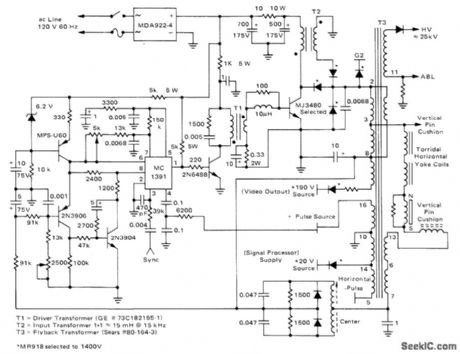
Self-regulating scan system includes short-circuit protection. Provides excellent high-voltage regulation at 25 kV. Vertical yoke current is also stabilized since it is powered from auxiliary fly-back winding. System consumes 30% less power than more conventional circuit using SCR half-wave regulated supply.-R. J. Valentine, A Self-Regulating Horizontal Scan System, Motorola, Phoenix, AZ, 1975, AN-750, p 7.
(View)
View full Circuit Diagram | Comments | Reading(1528)
10_V_WITH_MODERATE_DRIFT
Published:2009/7/15 22:10:00 Author:Jessie

Suitable for A/D converter applications in which output voltage can drift as much as 20 PPM/℃. Temperature-drift error is divided equally between zener and amplifier, permitting use of moderately low-drift components.-R. C. Dobkin, Don't Forget Reference Stability When Designing A-to-D Converters, EDN Magazine, June 20, 1977, p 105-108. (View)
View full Circuit Diagram | Comments | Reading(708)
10_V_WITH_TC_TRIMMlNG
Published:2009/7/15 22:09:00 Author:Jessie

Provides temperature-compensation trimming to give lowest possible reference-voltage drift for A/D converter. Reference zener is LM199A having 0.5 PPM/℃ drift that is independent of operating current. Low-drift combination of LM121 and LMl08A has drift predictably proportional to offset voltage, permitting use of potentiometers for trimming to better than 1 PPM/℃. Article gives details of trimming procedure to be used during temperature runs.- R. C. Dobkin, Don’t Forget Reference Stabillity When Desiging A-to-D Converters, EDN Magazine, June 20, 1977, p l05-108. (View)
View full Circuit Diagram | Comments | Reading(764)
S_SHAPED_RAMP
Published:2009/7/15 22:08:00 Author:Jessie
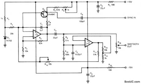
Developed for 60-Hz vertical deflection in high-resolution video display requiring highly linear ramp summed with second integral of ramp to give S shaping of deflection so sweep is linear on flat screen. Opamp A1 is connected as integrator that takes integral of constant voltage across zener D1. Period of integration is limited by UJT Q1 that resets integrating capacitor C1 when negative-going sync signal is applied to base 2 of Q1. Sawtooth linearity can be trimmed by adjusting ratio of R.4 to R5. Sync range is wide enough so external vertical hold can be eliminated. Amount of shaping can be adjusted with pot.-L. G. Smeins, S -Shaped Sawtooth Oscillator, EDN Magazine, Feb. 20, 1974, p 83 and 85. (View)
View full Circuit Diagram | Comments | Reading(1030)
65_V_REFERENCE
Published:2009/7/15 22:07:00 Author:Jessie

Reference amplifier uses mirror characteristic of noninverting input of current-mode opamp to determine zener current. Resulting voltage drop across zener provides, through R2, current reference for other or opamps or compensated voltage reference.-R. W Fergus, Use Current-Mode Op Amps in Reference Circuits, EDN Magazine, June 20, 1974, p 80 and 83. (View)
View full Circuit Diagram | Comments | Reading(721)
SOUND__IF__SUBSYSTEM
Published:2009/7/15 22:06:00 Author:Jessie
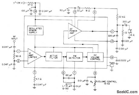
Single RCA CA1190GQ IC combines sound IF. FM detector. and complete audio amplifier for driving 8-16-or 32-ohm loudspeaker in TV receiver,Nominal power output is 3 W,Electronic volume control on chip provides improved taper with single 15K wire wound control,-“Linear Integrated Circuits and MOS/FETs,″RCA Solid-State Division. Somerville, NJ, 1977, p301 (View)
View full Circuit Diagram | Comments | Reading(915)
LOW_DRIFT_MICROPOWER
Published:2009/7/15 22:05:00 Author:Jessie

Uses JFET biased slightly below pinchoff in combination with micropower opamp to convert zero-temperature-coefficient drain current to correspondingly stable reference voltage. Additional JFET J2 makes operation independent of value of unregulated input. Output impedance is low. For higher output impedance, reference voltage can be taken from wiper of R2, but buffering could then be required. R1, is adjusted to compensate for temperature coefficient arising from opamp supply current.-N. Sevastopoulos and J. Mayer, Micropower Reference Stays Stable, EDN Magazine, Sept. 5, 1978, p 158. (View)
View full Circuit Diagram | Comments | Reading(834)
MICROPROCESSOR_SSTV_INTERFACE
Published:2009/7/15 22:05:00 Author:Jessie
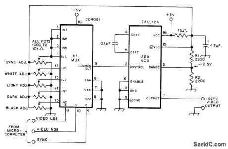
Digital-to-analog-to -frequency converter for slowscan television permits direct generation of simple graphic and alphameric characters by microprocessor, without use of camera, U1 is CD4051 CMOS analog multiplexor, and U2A is one section of 74LS124 TTL dual voltage-controlled oscillator. Picture format uses 64 different lines, repeated once to give total of 128 lines, with maximum of 64 different picture elements per horizontal line each having one of four shades of gray. Separate pot is provided for setting each of five different levels so VCO oscillates at proper frequencies: sync-1200 Hz; black-1500 Hz; dark-1767 Hz; light-2033 Hz; white-2300 Hz. Article covers operation in detail and gives flow diagrams for microprocessor subroutines required.-B. Sanderson, SSTV Pictures from Your Microcomputer, QST, Oct. 1978, p 25-29. (View)
View full Circuit Diagram | Comments | Reading(4452)
_66_V_WITH_741_OPAMP
Published:2009/7/15 22:04:00 Author:Jessie

Uses combination of negative and positive feedback to maintain constant current of 2 mA in D1, independent of variations in ambient temperature and unregulated input. Reference voltage of 6.6V, determined by breakdown voltage of 1N4611 zener, is scaled up to more positive level at output of A1. Scaled output has low impedance and can supply appreciable current without affecting reference voltage accuracy. Supply must be single-ended for reliable starting.-W. G. Jung, IC 0p-Amp Cookbook, Howard W. Sams, Indianapolis, IN, 1974, p 141-143. (View)
View full Circuit Diagram | Comments | Reading(0)
MODU_LATOR_MULTIPLIER
Published:2009/7/15 22:03:00 Author:Jessie
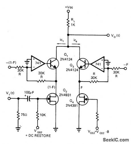
Balanced direct-coupled FET modulator/multiplier was developed for closed-circuit industrial color television system. Opamps handle modulation frequencies up to 1 MHz while providing linear response down to near zero modulation,-G. R. Shapiro, Analog Multipliers Offer Solutions to Video Modulation Problems, EDN Magazine, Sept. 1 1972, p 40-41. (View)
View full Circuit Diagram | Comments | Reading(1729)
VARIABLE_WIDTH_TO_1285_MHz
Published:2009/7/15 22:02:00 Author:Jessie

Single IC circuit uses two monostables to form pulse generator that covers over eight decades (0.054 Hz to 12.85 MHz) with only eight capacitors. Similarly, only eight capacitors cover pulse width range of over eight decades (60 ns to 18 s). Voltage control of frequency and pulse width can be obtained by connecting R2 and R4 to individual 1.5-4.5 V control voltage lines instead of to VCC. Frequency will then vary almost linearly with control voltage, while pulse width will vary almost inversely with control voltage. Capacitor values range from 1 pF to over 100 μF. -M. J. Shah, Wide-Range Pulse Generator Uses Single IC, EDN Magazine, Jan. 5, 1973, p 107 and 109. (View)
View full Circuit Diagram | Comments | Reading(1723)
CHROMA_SYSTEM
Published:2009/7/15 22:01:00 Author:Jessie
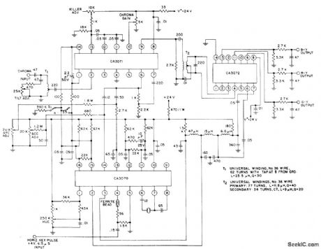
Uses RCA CA30T0 as subcarrier regenerator, CA3071 as chroma amplifier, and CA3072 as chroma demodulator, input can be taken from either first or second video stage of color TV receiver. Outputs from system are color difference signals for driving high-level amplifiers. Operates from single 24-V supply that should be maintained within 3 V. Only other requirement is 4-V 4.5-sμhorizontal keying pulse centered on color burst. Crystal oscillator generates 3.579545 MHz.- Linear Integrated Circuits and MOS/FET’s, RCA Solid State Division, Somerville, NJ, 1977, p 345-346. (View)
View full Circuit Diagram | Comments | Reading(1861)
SYNCHRONIZATION_TO_10_MHz
Published:2009/7/15 22:00:00 Author:Jessie

Free-running pulse generator circuit uses diode to inhibit operation until sync signal is applied. Circuit then pulses until sync signal returns to original state. Complementary outputs having pulse widths of 100 ns swing essentially from ground to power supply voltage that can be anywhere in range from 0.65 V to 15V. Values used for R and C determine frequency. For oscillation, R must be in range of 1 kilohm to 1 megohm. For 5-V supply, frequency is 1.2/RC.-B. Shaw, Oscillator Provides Fast, Low Duty-Cycle Pulses, EDN Magazine, March 20, 1975, p 73. (View)
View full Circuit Diagram | Comments | Reading(949)
VERTICAL_SYNC_SEPARATOR
Published:2009/7/15 21:58:00 Author:Jessie
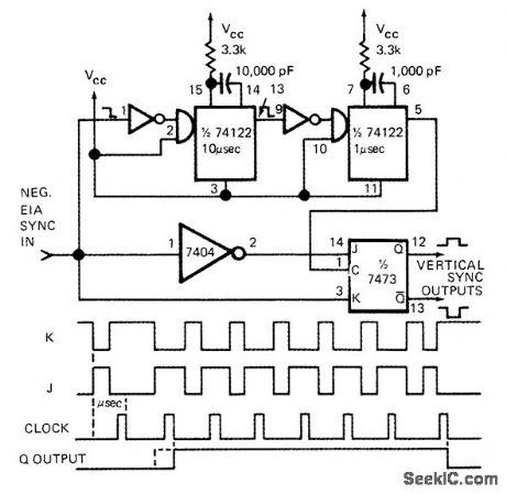
Arrangement uses controlled clocking sequence of JK flip-flop to detect presence of vertical sync interval in standard EIA television composite sync wave-form. Complementary sync waveforms J and K are fed to J and K inputs of 7473 flip-flop, which is clocked by 1-μs pulse that is delayed slightly longer than 10-μs horizontal sync interval. First clock pulse after 11-sμ interval changes flip-flop output Q to 1, where it stays for six clock periods before reverting to 0 state after vertical sync interval has passed.-W. G. Jung, Vertical Sync Separator Has No Integrating Network, EDN Magazine, Oct. 15, 1972, p 57. (View)
View full Circuit Diagram | Comments | Reading(3350)
| Pages:656/2234 At 20641642643644645646647648649650651652653654655656657658659660Under 20 |
Circuit Categories
power supply circuit
Amplifier Circuit
Basic Circuit
LED and Light Circuit
Sensor Circuit
Signal Processing
Electrical Equipment Circuit
Control Circuit
Remote Control Circuit
A/D-D/A Converter Circuit
Audio Circuit
Measuring and Test Circuit
Communication Circuit
Computer-Related Circuit
555 Circuit
Automotive Circuit
Repairing Circuit