
Circuit Diagram
Index 647
GAIN_PROGRAMMABLE_AMPLIFIER
Published:2009/7/14 3:14:00 Author:May

National AH5010 4-bit current-mode analog switch for TTL input is used with general-purpose opamp such as LM118 to give multiplying D/A converter at low cost. For CMOS control logic, use AM97C10 switch. Use of 10K for gain-programming resistor R gives compromise between switch resistance and switch leakage. Use 0.2% tolerance resistors for R and 2R, 0.5% for 4R, and 5% for highest resistance, with 0.1% tolerance for feedback resistor Rf which is also 10K, to give overall accuracy within 0.2%.-J. Maxwell, Analog Current Switch Makes Gain-Programmable Amplifier, Electronics, Feb. 17, 1977, p 99 and 101. (View)
View full Circuit Diagram | Comments | Reading(766)
PREFERRED_NONSATURATING_BISTABLE
Published:2009/7/15 6:00:00 Author:Jessie

Used for frequency division of pulse trains when high stability is required. Cascade connection with appropriate feedback can provide any desired ratio. Also useful for coding, gating, and synchronizing. Maximum operating rate is up to 1 Mc.-NBS, Handbook Preferred Circuits Navy Aeronautical Electronic Equipment, Vol. II, Semiconductor Device Circuits, PSC 15 (originally PC 253), p 15-2. (View)
View full Circuit Diagram | Comments | Reading(587)
16_30_MHz_20_W_HIGH_GAIN_DRIVER
Published:2009/7/14 3:13:00 Author:May

Broadband amplifier operating from 12-V supply uses Motorola MRF433 power transistors for class AB operation and MHW591 as predriver. For class A operation, power transistors should be MRF426. Q2 does not require heatsink because its peak dissipation is under 1 W. Power gain is 55 dB well beyond four-octave band of amplifier, and input VSWR is under 1.2.-H. 0. Granberg, Low-Distortion 1.6 to 30 MHz SSB Drivel Designs, Motorola, Phoenix, AZ, 1977, AN-779, p7.
(View)
View full Circuit Diagram | Comments | Reading(1979)
CATHODE_COUPLED_TRIGGER
Published:2009/7/15 5:58:00 Author:Jessie

Series diode improves sensitivity for cathode-coupled monostable mvbr while giving stability of 5% for threshold levels of several mv. Second tube can be triode, permitting use of 6U8 triode-pentode in compact assembly.-M. M. Vojinovic, Series Diode Increases Multivibrator Sensitivity, Electronics, 32:17, p 90-91. (View)
View full Circuit Diagram | Comments | Reading(632)
RELAY_MVBR_WITH_ISOLATOR_DIODES
Published:2009/7/15 5:56:00 Author:Jessie

Use of diodes to isolate capacitors reduces capacitance requirements for low frequencies. High-resistance relays for K2 and K3 cut costs.-R. L. lves, Multivibrator for Low Frequencies Uses Relays, Electronics, 34:32, p 166-169. (View)
View full Circuit Diagram | Comments | Reading(702)
VARIABLE_SWITCHING_FREQUENCY
Published:2009/7/14 3:12:00 Author:May

TL497 switching regulator operates at maximum frequency under maximum load conditions. For smaller loads, duty cycle is varied automatically by maintaining fixed ON time and varying switching frequency. Circuit optimizes efficiency at about 75% by reducing switching losses as load decreases.-J. Spencer, Monolithic Switching Regulators-They Fit Today's Power-Supply Needs, EDN Magazine, Sept. 5, 1977, p 117-121. (View)
View full Circuit Diagram | Comments | Reading(1796)
PULSE_WIDTH_MONITOR
Published:2009/7/15 5:45:00 Author:Jessie

Circuit turns on upper pilot lamp when pulse width is less than predetermined minimum value, because upper 7473 JK flip-flop is clocked when pulse falls to ground before 74121 mono recovers, triggering upper SCR on. Similarly, 8601 mono is set to coincide with specified maximum pulse width; if pulse falls to ground after this mono recovers, its JK flip-flop is clocked and lower (greater than) lamp is turned on. Fault indication is held until reset button is pushed.-J. Kish, Jr., Three ICs Monitor Pulse Width, EDN Magazine, March 20, 1973, p 86. (View)
View full Circuit Diagram | Comments | Reading(1814)
SIMPLE_FREQUENCY_SYNTHESIZER
Published:2009/7/14 3:11:00 Author:May

The 555 timer circuit is configured as a 10-kHz astable multivibrator that feeds this signal to the 4046 phase-locked-loop IC. The signal that is fed from this chip is then coupled to a divide-by-N counter. This counter will take the 10-kHz signal locked on by the 4046 and will produce multiples of the fundamental frequency(10 kHz). Therefore, it is possible to generate frequencies as high as 100 kHz with this circuit. When building this circuit, remember to use safety precautions when handling CMOS chips. (View)
View full Circuit Diagram | Comments | Reading(5484)
PULSE_EDGE_SELECTOR
Published:2009/7/15 5:37:00 Author:Jessie

Two quad TTL packages form simple circuit that generates output pulse at C as function of either leading or trailing edge of input pulse at A, depending on logic level at terminal D. Additional output at E supplies pulses coinciding with both leading and trailing edges of input, independently of logic level at D. Maximum input frequency is 10 MHz, and edge pulses are about 35 ns wide. IC1 is quad two-input EXCLUSIVE-OR gate, and IC2 is quad two-input NAND gate.-C. F. Reeves, A Programmable Pulse-Edge Selector, EDN Magazine, April 20, 1973, p 85 and 87. (View)
View full Circuit Diagram | Comments | Reading(689)
100_dB_DYNAMIC_RANGE
Published:2009/7/14 3:11:00 Author:May

Circuit generates log ratio of currents Ic1, and Ic2, with accuracy within 3% from 10 nA to 1 mA (100dB range) when Ic2 is fixed at 10-μA reference value. Accuracy increases to 1% for current inputs between 40 nA and 400 μA (80 dB). A2 supplies constant reference current to Q2.Q1 is operated as transdiode withQ2 providing temperature compensation of offset voltage.-W. G. Jung, IC Op-Amp Cookbook, Howard W. Sams, Indianapolis, IN, 1974 ,p 213-214. (View)
View full Circuit Diagram | Comments | Reading(662)
SENSE_AMPLIFIER
Published:2009/7/15 5:36:00 Author:Jessie
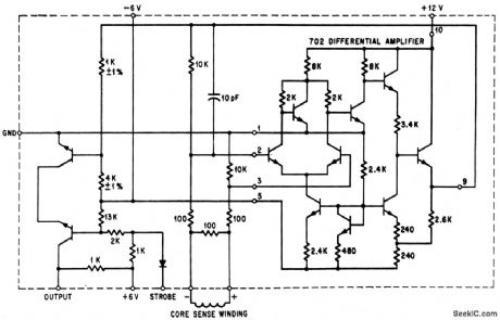
Uses two flatpacks (shaded areas)attached to thick-film passive network.-F. A. Plemenos. The packaging Revolution, Part VI: Converting to Microelectronics. Electronics.39:4,p103-109. (View)
View full Circuit Diagram | Comments | Reading(925)
5_V_40_A_20_kHz_SWITCHED_MODE
Published:2009/7/14 3:11:00 Author:May

Uses Motorola 2N6544 power transistors operating with 3-A collector current (other half of power stage is identical). Bridge rectifier and capacitive filter connected directly to AC line form 150-VDC sup-ply for inverter operating at 20 kHz. Regulators MC7806 and MC7906 operating from MDA9221 bridge rectifier of 15-W filament transformer T3 provide ±6 V for logic circuits that provide pulse-width modulation for inverter. When logic signal is high, MPS-U51 saturates and supplies 1 A to base of 2N6544 inverter power transistor When logic is low, MPS-U95 Darlington holds inverter transistor off.-R. J. Haver, Switched Mode Power Supplies-Highlighting a 5-V, 40-A Inverter Design, Motorola, Phoenix, AZ, 1977, AN-737A, p 10. (View)
View full Circuit Diagram | Comments | Reading(1374)
WIDE_DYNAMIC_RANGE_DIFFERENTIAL_AMPLIFIER
Published:2009/7/15 5:34:00 Author:Jessie
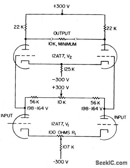
Used in amplifying and measuring small differences between two large voltages, either of which may be up to 100V above ground. Amplification of difference voltage is 250. Frequency response is within 3 db from d-c to 250 kc.-D. D. Davis, High Dynamic Range Differential Amplifier, Electronics, 31:5, p 64-66. (View)
View full Circuit Diagram | Comments | Reading(684)
THREE_TONE_GENERATOR
Published:2009/7/14 3:10:00 Author:May

The three-tone generator makes a great warning device. It has a lot of uses; for example, if the appropriate switch is used for S1, the circuit can be used as a burglar alarm. When S1 is pressed, it turns on the circuit. The tone frequencies depend on resistor R1 and capacitors C1 through C3.Switch S2 lets you select between those capacitors. Capacitor C1 produces the highest frequency because it has the lowest capacitance, while C3 generates the lowest frequency. (View)
View full Circuit Diagram | Comments | Reading(954)
COMPLETING_LAST_CYCLE
Published:2009/7/15 5:34:00 Author:Jessie

Developed for applications requiring that gated oscillator must always complete its timing cycle. Circuit uses only two NAND gates and two diodes, none of which are critical as to type. With no input at A, oscillator output B is low. When A is driven high, D goes low initially and drives output B high. If input at A is removed, regenerative feedback is applied from B through diode D2 to C until normal timing cycle is finished. Then, with B low, D becomes high and keeps output B low.-L. P. Kahhan, Gated Oscillator Completes Last Cycle, EDN Magazine, Jan. 5, 1977, p 43. (View)
View full Circuit Diagram | Comments | Reading(626)
ENCODER
Published:2009/7/14 3:09:00 Author:May

Used between fransfluxor and digital shift register of converter that changes analog inputs to six-bit binary Gray code.-N. Aron and C. Granger, Analog-To-Digital Converter Uses Transfluxors,Electronics,35:20,p 62-66. (View)
View full Circuit Diagram | Comments | Reading(801)
DIFFERENTIAL_CURRENT_AMPLIFIER
Published:2009/7/15 5:33:00 Author:Jessie

Uses eight npn transistors and eight diodes.-D. D. Robinson, Linear Microcircuits Scarce? Now You Can Breadboard Your Own, Electronics, 37:27, p. 58-64. (View)
View full Circuit Diagram | Comments | Reading(671)
EMOTE_TELEPHONE_RINGER
Published:2009/7/14 3:09:00 Author:May

When there is no ring signal, the phone line's on-hook voltage (about 50 V) keeps the triac (Radio Shack 276-1001 or equivalent) from switching on, so the optocoupler doesn't conduct. When the phone rings, terminal 4 of the optocoupler feeds pulses through R3 and R4 to the gate of SCR1. The activated SCR connects the bell to the 12-V supply. Pulses are about 400 Hz, so the bell might sound a bit rough. The opening of the bell's breaker points cuts the thyristor's holding current to stop it from conducting when the gate signal stops. A 12-V, 2-A power supply operates the unit. Adjust R3 high enough so that the SCR is not triggered between rings, but low enough to trigger it when the phone is ringing. (View)
View full Circuit Diagram | Comments | Reading(1959)
11X_PULSE_STRETCHER
Published:2009/7/15 5:33:00 Author:Jessie
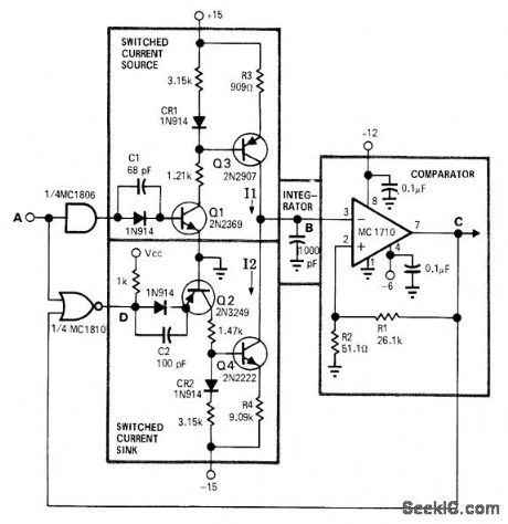
Provides negative output pulse width equal to positive input pulse multiplied by 1 + R4/R3, which is 11 for values shown. Output pulses are TTL-or DTL-compatible. Minimum output pulse width is 70 ns, and maximum is 1/11 of pulse repetition rate. Circuit consists of switched current source, switched current sink, integrating capacitor, and comparator. Q1 and Q2 act as switches for current sources Q3 and Q4, while C1 and C2 reduce turn-on and turnoff times of switches. CR1 and CR2 provide temperature compensation for Q3 and Q4. AND gate compensates for propagation delay in NOR gate, to ensure that current sink is switched on by trailing edge of input pulse. Add inverter if output must be same polarity as input.-F. Tarico, Linear Circuit Multiplies Pulse Width, EDN|EEE Magazine, Dec. 1, 1971, p 45-46. (View)
View full Circuit Diagram | Comments | Reading(704)
FOUR_STAGE_DIFFERENTIAL_AMPLIFIER
Published:2009/7/15 5:29:00 Author:Jessie

Designed for maximum open-loop amplification of differential signal. Series-shunt negative feedback provides high input impedance and low output impedance. Responds to differential signal of 25 microvolts superimposed on common level that varies from 0 to 5V. Voltage gain is continuously variable from 100 to 500. Frequency response is flat within 1% from d-c to 1,000 cps. Ideal for telemetering systems.-Texas Instruments Inc. Transistor Circuit Design, McGraw-Hill, N. Y., 1963, p 138. (View)
View full Circuit Diagram | Comments | Reading(863)
| Pages:647/2234 At 20641642643644645646647648649650651652653654655656657658659660Under 20 |
Circuit Categories
power supply circuit
Amplifier Circuit
Basic Circuit
LED and Light Circuit
Sensor Circuit
Signal Processing
Electrical Equipment Circuit
Control Circuit
Remote Control Circuit
A/D-D/A Converter Circuit
Audio Circuit
Measuring and Test Circuit
Communication Circuit
Computer-Related Circuit
555 Circuit
Automotive Circuit
Repairing Circuit