
Circuit Diagram
Index 650
152_165_MHz_TO_14694_MHz
Published:2009/7/15 5:16:00 Author:Jessie

Permits listening to public service band with any good 2-meter FM receiver or transceiver. Local oscillator has tuning range of 7-8 MHz and uses germanium PNP high-frequency transistor. No RF stage is needed for full quieting from stations 10 miles away when using ground-plane antenna. To avoid burning out convener, do not transmit while converter is connected to transceiver. Article gives coil-winding data. -H. Schoenbach, Public Service Band Converter, 73 Magazine, Dec. 1974, p 78-79 (View)
View full Circuit Diagram | Comments | Reading(2011)
VARIABLE_TRANSCONDUCTANCE_DIVIDER
Published:2009/7/14 2:55:00 Author:May
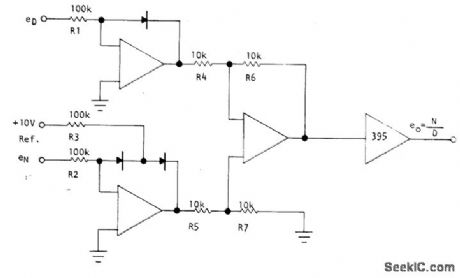
Practical analog divider follows ideal division equation over typical 20:1 range of reference current and operates in two quadrants. Circuit is analyzed in terms of logarithmic behavior of its elements. Bandwidths up to 5 MHz can be achieved. Article gives design equations.-L.Counts and D. Sheingold, Analog Dividers: What Choice Do You Have?, EDN Magazine, May 5, 1974, p 55-61. (View)
View full Circuit Diagram | Comments | Reading(784)
28_MHz_TO_144_MHz
Published:2009/7/15 5:15:00 Author:Jessie
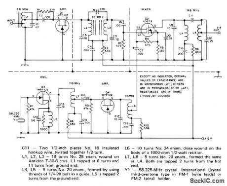
Addition of small upconverter, between 145.85 and 145.95 MHz, is fed verter to 144-MHz (2-meter) SSB transceiver to antenna terminal of receiver.-T. McMullen, permits reception of 10-meter signals from An Up Converter for Oscar Reception, QST, Oscar satellite on single transceiver. Output of March 1975, p 41-44. (View)
View full Circuit Diagram | Comments | Reading(2502)
10_W_FOR_220_MHz
Published:2009/7/14 2:54:00 Author:May
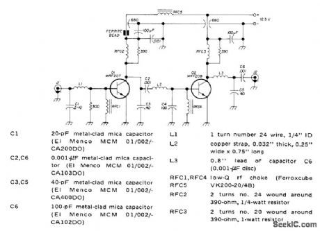
Class C RF power amplifier for VHF FM transmitter has stable gain of 20 dB for operating bandwidth of 40 MHz. Article gives design procedure using Smith chart and covers construction and tune-up.-J. DuBois, 220-MHz BF Power Amplifier for VHF FM, Ham Radio, Sept. 1973, p 6-8. (View)
View full Circuit Diagram | Comments | Reading(2789)
SEQUENTIAL_PULSES
Published:2009/7/15 5:15:00 Author:Jessie
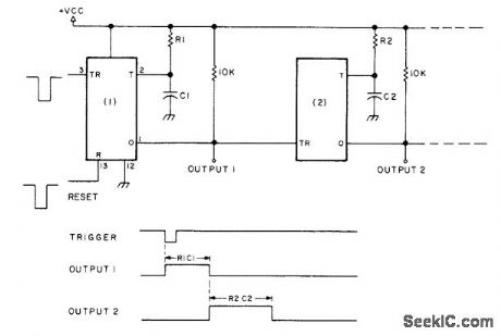
Any number of sections of 554 quad monostable timer can be cascaded as shown to give sequential series of output pulses of widths determined by values of R and C. No coupling capacitors are required because timer is edge-triggered. Negative reset pulse simultaneously resets all sections. Varying control voltage (in range of 4.5-16V) affects period of all timer sections simultaneously.-H.M. Berlin, IC Timer Review, 73 Magazine, Jan.1978, p 40-45. (View)
View full Circuit Diagram | Comments | Reading(532)
VIDEO_PROCESSOR
Published:2009/7/14 2:53:00 Author:May
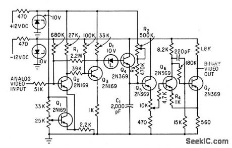
Analog video input from closed-circuit tv microscope is converted to binary video output by difference amplifier Q1-Q2, squaring amplifier Q3, pulse shaper Q4, and emitter-follower Q5 which buffers R-C network from Schmitt trigger Q6-Q7.-N. F. Izzo and W. Coles, Blood-Cell Scanner Identifies Rare Cells, Electronics, 35:17, p 52-57. (View)
View full Circuit Diagram | Comments | Reading(694)
5_V_FIXED_OFF_TIME_SWITCHING
Published:2009/7/14 2:53:00 Author:May

Uses LM305 regulator and Unitrode hybrid power switch in PIC600 series. Operates in fixed OFF-time mode. Output ripple of 100 mV P-P is independent of input voltage range of 20 to 40 V for output of +5 V ±1%. Switching speed is nominally 50 kHz but can go up to 100 kHz. Article covers theory of operation in detail.-L. Dixon and R. Patel, Designers' Guide to: Switching Regulators, EDN Magazine, Oct. 20, 1974, p 53-59. (View)
View full Circuit Diagram | Comments | Reading(644)
PHONE_IN_USEINDICATOR
Published:2009/7/14 2:52:00 Author:May
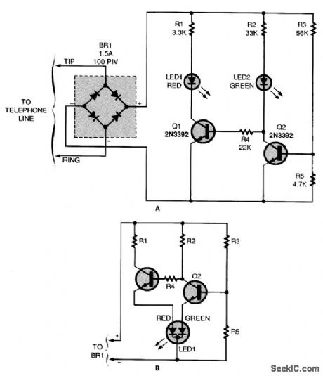
Tired of having your phone calls interrupted by others picking up the receiver? This circuit (A) will show others when the phone is in use. If you would like to experiment with a tricolor LED, check out the optional schematic (B).
When all telephones are on-hook, Q2's base is turned on by a voltage-divider circuit, consisting of R3 and R5. (The value shown for R5 causes the device to switch over at about 9 V; it can be changed to facilitate other voltage levels.) Transistor Q2 allows current to flow through R2 and LED2, indicating that the phone line is not in use. It also effectively grounds the base of Q1 and forces LED1 to remain off. When the voltage drops because a telephone goes off-hook, Q2 stops con-ducting, which allows a little current to flow from R2, LED2, and R4 to Q1's base. When that occurs, Q1 conducts, energizing LED1 and LED2 is deprived of sufficient current to glow. The bridge rectifier compensates for a possible reversal between the tip and ring wires, and rectifies the ring signal. (View)
View full Circuit Diagram | Comments | Reading(613)
UJT_CONVERTER_FOR_ACCELEROMETER
Published:2009/7/14 2:52:00 Author:May
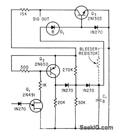
Converts digital output to voltage analog that indicates rate of acceleration or, when bleeder resistor is removed, actual distance traveled.-F. W. Kear, Unijunction Transistor Pulse-Circuit Design, Electronics, 35:21,p 58-60. (View)
View full Circuit Diagram | Comments | Reading(691)
_5_V_SWITCHING_AT_10_A
Published:2009/7/14 2:52:00 Author:May

Uses Unitrode PIC635 hybrid power switch with LM304 regulator for switching speeds up to 100 kHz with input voltage range of 20-40 V. 01 provides cur-rent-limiting action.- Switching Regulator Design Guide, Unitrode, Watertown, MA, 1974, U-68A, p 9. (View)
View full Circuit Diagram | Comments | Reading(0)
ELEVEN_BIT_DECODER
Published:2009/7/14 2:50:00 Author:May

Well-regulated transistor power supply and binary-weighted network of precision wire-wound resistors give high-precision conversion of 11-bit digital value to current analog. Output goes to magnetic modulator. Regulated 320-v supply(not shown) uses silicon junction diodes in full-wave bridge, with silicon zener diode as reference.-N. Aron,Precise Converter Takes Current Analog of Digital Voltage Pulses, Electronics,35:32, p 68-71. (View)
View full Circuit Diagram | Comments | Reading(1032)
COLOR_BAR_GENERATOR
Published:2009/7/15 5:15:00 Author:Jessie

National MM5322 chip forms complete dot-bar and color hue generation system. Chip divides internal crystal-controlled oscillator frequency to provide timing, sync, and video information required for aligning color TV receivers. Composite video output serves for complete black-and-white dot-bar operation to give variety of screen patterns. Separate output is provided for precise gating of 3.56-MHz color bursts.- MOS/LSI Databook, National Semiconductor, Santa Clara, CA, 1977, p 4.18-4-22. (View)
View full Circuit Diagram | Comments | Reading(0)
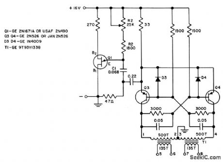
TRANSFORMER_WINDING_SPEEDS_SWITCHING
Published:2009/7/15 5:13:00 Author:Jessie

Addition of speed-up winding N1 to con ventional transformer orrangement of inverler, with C1 in series with N1, increases switching speed. Clipping of resulting base-collector voltage spikes is provided by net work D1-D2-C2-R3.-A. G. Lloyd, Speed4Jp Circuits Improve Switching of Transistor Inverters, Electronics, 34:45, p 92-94. (View)
View full Circuit Diagram | Comments | Reading(650)
GENERAL_PURPOSE_VIDEO_SWITCH
Published:2009/7/15 5:12:00 Author:Jessie

When used for switching TV cameras.DG200 CMOS analog switch provides 45-dB isolation at 10 MHz between on and off cameras,Insertion loss of switches 0.5 dB, For greater isolation、use additional analog switch in each camera line.-Analog Switches and Their Applications ” Siliconix. Santa Clara,CA,1976.p 7-70. (View)
View full Circuit Diagram | Comments | Reading(1564)
175_kHz_TO_1515_OR_3515_kHz
Published:2009/7/15 5:12:00 Author:Jessie
Crystal-controlled VLF converter covering 1750-meter band gives choice of two outputs, selected by S2, for communication or broadcast receiver. Tuning range is 160 to 190 kHz. Connect general-coverage receiver to IF output terminals with length of coax. -J. V. Hagan, A Crystal-Con-trolled Converter and Simple Transmitter for 1750-Meter Operation, QST, Jan. 1974, p 19-22. (View)
View full Circuit Diagram | Comments | Reading(2398)
96_MILLISEC_PULSE_STRETCHER
Published:2009/7/15 5:10:00 Author:Jessie

Monostable multivibrator stays on for 96 millisec after Schmitt trigger goes off, while C discharges through R12. -J. R. Giroux, Multi's Output Duration Controlled by Input, Electronics, 38:4, p 88-89. (View)
View full Circuit Diagram | Comments | Reading(791)
UNITY_GAIN_INVERTER
Published:2009/7/15 5:10:00 Author:Jessie
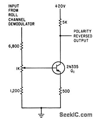
Provides for differential roll motion of missile autopilot.-J. H. Porter, Miniaturized Autopilot System for Missiles, Electronics, 33:43, p 60-64. (View)
View full Circuit Diagram | Comments | Reading(697)
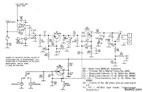
WWV_CONVERTER
Published:2009/7/15 5:08:00 Author:Jessie

Designed for use with amateur receiver for reception of NBS stationsWWV or WWVH on 10, 15, or 25 MHz. Receiver is tuned to 4, 14, or 21 MHz to serve as IF amplifier, detector, and audio stages. Current drain of converter is 15 mA, low enough for operation from 9-V transistor-radio battery. Table gives tuned-circuit values for frequency desired. Restriction to single frequency eliminates band-switching. Q1 can be any commom-gate JFET RF amplifier providing 8-dB gain. Mixer is 40673 MOSFET. Oscillator transistor is not critical. Oscillator output serves for all three WWV frequencies. -C. Watts, NBS-Ears for Your Ham-Band Receivers, QST, June 1976, p 25-26. (View)
View full Circuit Diagram | Comments | Reading(0)
16_W_4003200_CPS_SQUARE_WAVE_INVERTER_DRIVE
Published:2009/7/15 5:07:00 Author:Jessie
Uses transistor mvbr with unijunction transistor to stabilize and control frequency Efficiency is 85%. Has good fro. quency stability. Square-wave outputs are used lo drive d-c to a-c inverter. - Transistor Manual, Seventh Edition, General Electric Co., 1964, p 236. (View)
View full Circuit Diagram | Comments | Reading(1156)
TRANSFORMER_CONTROLLED__MVBR
Published:2009/7/15 5:06:00 Author:Jessie
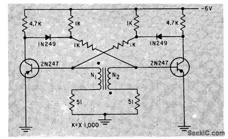
Gives sharper trailing edges und tighter control over ratio of on times of the two sides, as compared to choke control for same free-running mvbr. -W. M. Carey, Using Inductive Control in Computer Circuits, Electronics, 32:38, p 31-33. (View)
View full Circuit Diagram | Comments | Reading(526)
| Pages:650/2234 At 20641642643644645646647648649650651652653654655656657658659660Under 20 |
Circuit Categories
power supply circuit
Amplifier Circuit
Basic Circuit
LED and Light Circuit
Sensor Circuit
Signal Processing
Electrical Equipment Circuit
Control Circuit
Remote Control Circuit
A/D-D/A Converter Circuit
Audio Circuit
Measuring and Test Circuit
Communication Circuit
Computer-Related Circuit
555 Circuit
Automotive Circuit
Repairing Circuit