
Circuit Diagram
Index 648
POLARITY_DETECTOR
Published:2009/7/14 3:07:00 Author:May

Q1-Q2 amplify negative analog samples greater than 100 mv, to provide sharp pulse output for driving monostable mvbr in analog-digital converter.-N, Aron and C, Granger, Analog-To-Digital Converter Uses Transfluxors Electronics, 35:20, p 62-66. (View)
View full Circuit Diagram | Comments | Reading(868)
REMOTE_TELEPHONE_BELL_RINGER
Published:2009/7/14 3:06:00 Author:May

The telephone-line extension bell ringer shown will enable you to add a remote ringer in your garage or some other area where a ringing telephone cannot be heard Up to Four ringers can be used on a single telephone line, and a remote bell can be used 100 feet or more away from the unit.By substituting a light bulb for T2 and dispensing with the bell,the circuit can be made useful for the hearing-impaired.About 50 to 60 V dc is present between the tip and ring (red and green) wires of an unoccupied telephone line.Capacitor C1 blocks that dc voltage.The MOV just shunts any dialing pulses generated by a rotary phone that might be on the same line To make the phone ring,the tip and ring wires deliver an ac signal of between 90 and 130 V to the phone That ac signal is coupled through C1 to the neon lamps,NE1 and NE2 Those neon bulbs provide line isolation between the unit and the telephone line. They also neon fire (ionize) when more than 100 V is present on the phone line (in other words, during the ring signal). When they fire, they form a three-step voltage divider with the bridge rectifier. The voltage across the bridge is rectified, then filtered by R1, R2, C2, and C3, and causes Q1 to conduct. Then pins 2 and 6 of U1 go low, causing pin 3 of U1 to go high. The optoisolator and triac then turn on, applying power to the remote bell through a doorbell transformer (T2). (View)
View full Circuit Diagram | Comments | Reading(1933)
PHASE_INVERTER_FOR_CODE_CONVERTER
Published:2009/7/15 5:29:00 Author:Jessie

In addition to phase reversal of input signal, single npn transistor provides isolation between negative input pulse and core driver, which is Schmitt trigger having discrimimation level within 10% of -4.5 v including phase inverters. Signals below that level are disregarded. Signal range from 6 to 12 v will cause pulse output from Schmitt, with duration dependent on duration of input signal. When Schmitt trigger emits pulse, 1N704 driver supplies 30-ma current pulse, writing a ONE into ifs associated core.-R. Wasserman und W. Nutting, Solid-Stale Digital Code-to-Code Converter, Electronics,32:50, p 60-63. (View)
View full Circuit Diagram | Comments | Reading(725)
150_KC_BISTABLE
Published:2009/7/15 5:29:00 Author:Jessie

Designed as storage element in digital logic circuits for computer, control, and communication equipment. Can be used as counter and as serial or parallel shift register at operating rates up to 150 kc under maximum load. Article gives connections of lettered terminals for various circuit functions and performance characteristics.-NBS, Handbook Preferred Circuits Navy Aeronautical Electronic Equipment, Vol. II, Semiconductor Device Circuits, PSC 9 (originally PC 212), p 9-2. (View)
View full Circuit Diagram | Comments | Reading(589)
STEPPING_5_V_UP_TO_15_V
Published:2009/7/14 3:05:00 Author:May

Fairchild μA78S40 switching regulator transforms 5 V to 15 V at efficiency of 80% for 150-mA load. Average input current is only 550 mA. Article gives de-sign equations.-R. J. Apfel and D. B. Jones, Universal Switching Regulator Diversifies Power Subsystem Applications, Computer Design, March 1978, p 103-112. (View)
View full Circuit Diagram | Comments | Reading(498)
10_MICROSEC_MONOSTABLE_MVBR
Published:2009/7/15 5:28:00 Author:Jessie

Output pulse width is approximately 10 microsec with values shown for basic one-shot. -Texas Instruments Inc., Transistor Circuit Design, McGraw-Hill, N.Y., 1963, p 381. (View)
View full Circuit Diagram | Comments | Reading(833)
COMPUTE_AMPLIFIER
Published:2009/7/14 3:05:00 Author:May
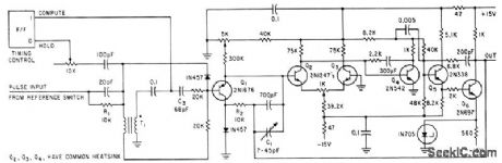
Converts digital output of reference switch for switch decoder to equivalent analog voltage and holds voltage for transfer to hold amplifier.-R. M, Centner and J. R. Wilkinson, New Approach to Serial Decoding Eliminates Static Storage, Electronics, 35:34, p 32-35. (View)
View full Circuit Diagram | Comments | Reading(520)
DIFFERENTIAL_AMPLIFIER
Published:2009/7/15 5:27:00 Author:Jessie
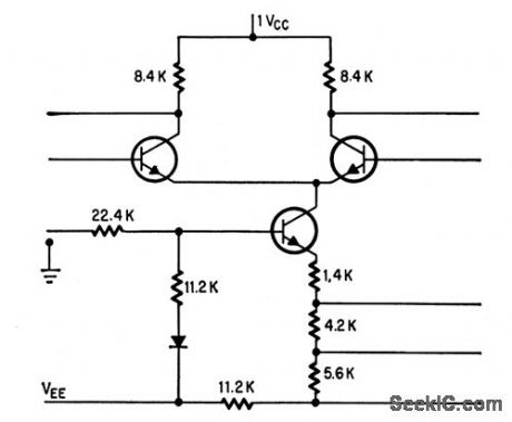
Use of transistor in place of emitter resistor gives tenfold increase in impedance of emitter circuit, up to 200,000 ohms, while using only 1% of substrate area that would be needed by film resistor of this size.-R. Hirschfeld, IC's lmprove Differential Amplifiers-and Vice Versa, Electronics, 38:16, p 75-79. (View)
View full Circuit Diagram | Comments | Reading(0)
LOW_COST_USING_OPAMP
Published:2009/7/14 3:03:00 Author:May
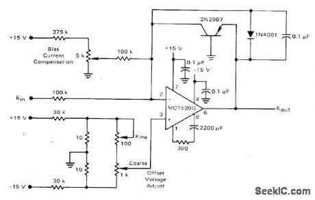
Motorola MC1539G opamp is connected with PNP transistor as logarithmic element. Circuit requires external compensation, has about 200-nA bias current, and accommodates wide range of input voltages when appropriate networks are used to compensate for errors. To adiust bias current initially, replaee transistor with 500K resistor and ad just 5K pot for gain of 5 over input signal range.-K. Huehne, Transistor Logarithmic Conversion Using an Integrated Operational Amplifier, Motorola, Phoenix, AZ, 1971, AN-261A, p 4. (View)
View full Circuit Diagram | Comments | Reading(722)
UNITY_GAIN_DIFFERENTIAL_D_C_AMPLIFIER
Published:2009/7/15 5:26:00 Author:Jessie

Negative feedback with differential input and single-ended output give gain stability of 1.0000 for output of 1.2V across 100-ohm load, for use in battery-powered transistor leakage-current tester.-A. T. Ashby, T. R. Shaifer, and H. R. Hegner, Testing Transistors In.-Circuit, Electronics, 37:17, p 53-56. (View)
View full Circuit Diagram | Comments | Reading(883)
_10V_SWITCHING
Published:2009/7/14 3:03:00 Author:May

Uses LM304 regulator and Unitrode hybrid power switch in PIC600 series to provide output of 10 A. R1 and R2 determine reference voltage. Current limiting is achieved by reducing reference voltage to ground instead of turning off base drive to power output switch. Article covers operating theory.-L. Dixon and R. Patel, Designers' Guide to: Switching Regulators, EDN Magazine, Oct. 20, 1974, p 53-59. (View)
View full Circuit Diagram | Comments | Reading(811)
PREFERRED_PRF_GENERATOR
Published:2009/7/15 5:26:00 Author:Jessie

Astable plate-to-grid coupled mvbr serves as moderately stable repetition-rate generator having greater frequency stability than blocking oscillator and fewer components than Wien-bridge oscillator. One drawback is that output impedance for positive pulses equals plate load resistance, which must be relatively high for good frequency stability. Output is 260 V for 5814A and 125 V for 6111. Maximum prf is 8,000 pps.-NBS, Handbook Preferred Circuits Navy Aeronautical Electronic Equipment, Vol. I, Electron Tube Circuits, 1963, PC 40, p 40-2. (View)
View full Circuit Diagram | Comments | Reading(617)
FET_VOLTAGE_COMPARAIOR
Published:2009/7/14 3:03:00 Author:May

Circuit uses spdt configuration. Used to switch reference voltage (such as ground) to successive points on binary voltage ladder until comparator determines that output of ladder is equal to that of unknown voltage. Sine and square wave inputs at A and B produce output at C. Used also for low-level differential switching.-J. Gulbenk and T. F. Prosser, How Modules Make Complex Design Simple, Electronics, 37:32, p 50-54. (View)
View full Circuit Diagram | Comments | Reading(613)
SIMPLE_WIDEBAND_NOISE_GENERATOR
Published:2009/7/14 3:03:00 Author:May

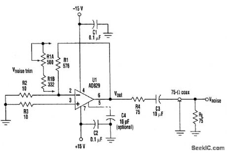
This relatively simple op-amp noise generator amplifies the input voltage noise of a wideband, decompensated op amp. If a device with a single-gain stage is selected, the output noise will be spectrally flat up to the closed-loop bandwidth. The op amp is manufactured by Analog Devices Inc. (View)
View full Circuit Diagram | Comments | Reading(1551)
INVERTER_REFERENCE_ELEMENT
Published:2009/7/15 5:23:00 Author:Jessie

Accuracy and stability of d-c to 400-cps a-c inverter are achieved by temperature compensation of IN2169A zener reference element. Silicon transistors are used where d-c levels are handled.-R. Wileman, linear Circuits Regulale Solid-Stale Inverler, Electronics, 33:16, p 61-63. (View)
View full Circuit Diagram | Comments | Reading(646)
PROGRAMMABLE_FREQUENCY_STATE_VARIABLE
Published:2009/7/14 3:03:00 Author:May

Provides choice of low-pass, high-pass, and bandpass out puts with logic-selectable center frequency of 700 or 7000 Hz. Logic input controls DG307 low-power dual analog switch for changing values of frequency-determining resistors R1 and R2.-″Analog Switches and Their Applications,″Siliconix, Santa Clara,CA,1976, p 7-86. (View)
View full Circuit Diagram | Comments | Reading(678)
144_MHz_TO_28_MHz
Published:2009/7/15 5:22:00 Author:Jessie
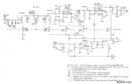
Brings 2-meter band to input range of ordinary amateur receiver. Crystal eliminates need for multiplier stages that can generate spurious responses. Signal can be injected from external source if crystal is re moved. -Construction Hints for VHF Converters, QST, Sept. 1975, p 32-33 and 39. (View)
View full Circuit Diagram | Comments | Reading(1660)
40_dB_LOGAMP
Published:2009/7/14 3:02:00 Author:May

Uses Optical Electronics 2457 logarithmic module containing two pairs of bipolar log elements and three opamps. Connection shown produces pure tog10 function on positive inputs. Zero point is set by R2 or by reference e. Reference must be positive for pos-tive logs and negative for negative logs. Trim 110K resistors for exactly 10-V output,- Two-Decade Precision Logarithmic Amplifior, Optical Electronics, Tucson, AZ, Applicatlon Tip 10212. (View)
View full Circuit Diagram | Comments | Reading(607)
TUNNEL_DIODES_READ_5_APERTURE_CORE
Published:2009/7/14 3:02:00 Author:May

Circuit also controls switching of binary weighted current generators used in analog-digital converter. W. G. Trabold, Tunnel Diodes Save Parls-Continuous Readout of Magnetic Cores, Electronics, 36:36, p 38-39. (View)
View full Circuit Diagram | Comments | Reading(643)
WEIGHTING_CIRCUIT
Published:2009/7/14 3:00:00 Author:May

Circuit introduces precise amount of current into point P within few nsec in response to output of threshold tunnel diode, contributing to accurate conversion of wideband analog signals into 64 levels that are described by six bits of binary language.-H. R. Schindler, Semiconductor Circuits in a UHF Digital Converter, Electronics, 36;35, p 37-40. (View)
View full Circuit Diagram | Comments | Reading(728)
| Pages:648/2234 At 20641642643644645646647648649650651652653654655656657658659660Under 20 |
Circuit Categories
power supply circuit
Amplifier Circuit
Basic Circuit
LED and Light Circuit
Sensor Circuit
Signal Processing
Electrical Equipment Circuit
Control Circuit
Remote Control Circuit
A/D-D/A Converter Circuit
Audio Circuit
Measuring and Test Circuit
Communication Circuit
Computer-Related Circuit
555 Circuit
Automotive Circuit
Repairing Circuit